PI5PD2041B/51B
70mΩ Current-Limited, Power-Distribution Switches
|||||||||||||||||||||||||||||||||||||||||||||||||||||||||||||||||||||||||||||||||||||||||||||||||||||||||||||||||||||||||||||||||||||||||||||||||||||||||||||||||||||||||||||||||||||||||||||||||||||||||||||||||||||||||||||||||||||||||||||||||||||||||||||||||||||||||||||||||||||||||||||||||||||||||||||||||||||||||||||||||||||||||||||||||||||||||||||||||||||||||||||||||||||||||||||||||||||||||||||||||||||||||||||||||||||||||||||||||||||||||||||||||||||||||||||||||||||||||||
Features
Description
x
x
x
x
x
x
x
x
x
x
x
x
The PI5PD2041B/51B is an integrated 70mΩ N-channel
MOSFET power switches for self-powered and buspowered Universal Series Bus (USB) applications. The
devices are equipped with charge pump circuitry to drive
the internal MOSFET switch. The switch’s low RDS(on),
70mΩ meets USB voltage drop requirements. This
power-distribution switch is designed to set current limit
at 1.0A typically.
When the output load exceeds the current-limit threshold
or a short-circuit situation is present, the devices limit
the output current by switching into a constant-current
mode, pulling the over-current (/OC) logic output low.
When continuous heavy overloads and short-circuits
increase the power dissipation in the switch, causing the
junction temperature to rise, a thermal protection circuit
turns off the switch to prevent damage. Recovery from a
thermal shutdown is automatic once the device has
cooled sufficiently. Internal circuitry ensures that the
switch remains off until valid input voltage is present..
70mΩ High-Side MOSFET
0.5A Continuous Current
Thermal and Short-Circuit Protection
Accurate Current Limit (1.0A typ.)
Operating Range: 2.7V to 5.5V
0.6ms Typical Rise Time
Under-Voltage Lockout
Deglitched Fault Report (/OC)
1μA Maximum Standby Supply Current
Reverse Current Blocking
Ambient Temperature Range: -40°C to 85°C
UL Recognized, File Number E341484
Applications
x
x
x
x
x
x
Laptop, Motherboard PC
USB Bus/Self Powered Hubs
TV and Set-top BOX Power switch
USB Peripherals
Battery-Powered Equipment
Hot-Plug Power Supplies
Pin Description
Pin No.
2
5
Pin Configuration
287
�
*1'
�
�
4
,1
4
3
�2&
�
�
�(1
1
Pin
Type
Description
GND
- Ground.
IN
I Power Input Voltage.
/EN
Chip Enable, logic low turns
I
(PI5PD2041B)
on power switch.
EN
Chip Enable, logic high turns
I
(PI5PD2051B)
on power switch.
Over current, open-drain
/OC
O
output, active-low.
OUT
O Power Output Voltage
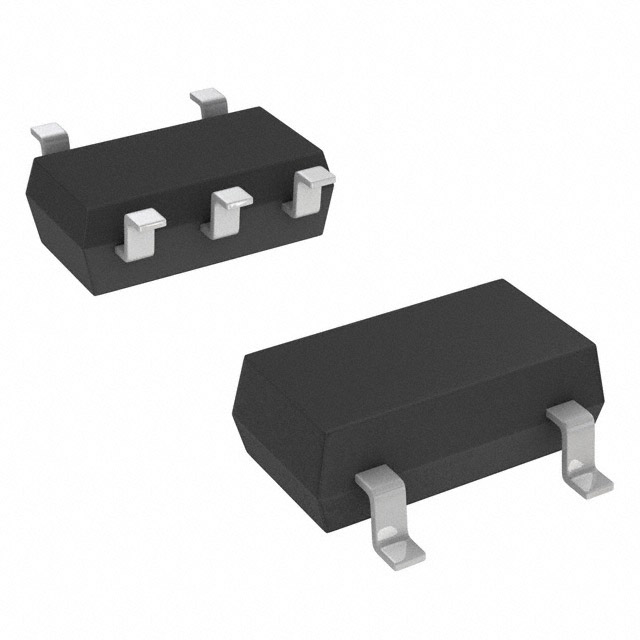
PI5PD2041B SOT23-5 (Top View)
287
�
*1'
�
�2&
�
�
,1
�
(1
PI5PD2051B SOT23-5 (Top View)
2013-07-0009
PT0317-5
1
07/31/13
�PI5PD2041B/51B
70mΩ Current-Limited,
Power-Distribution Switches
|||||||||||||||||||||||||||||||||||||||||||||||||||||||||||||||||||||||||||||||||||||||||||||||||||||||||||||||||||||||||||||||||||||||||||||||||||||||||||||||||||||||||||||||||||||||||||||||||||||||||||||||||||||||||||||||||||||||||||||||||||||||||||||||||||||||||||||||||||||||||||||||||||||||||||||||||||||||||||||||||||||||||||||||||||||||||||||||||||||||||||||||||||||
Functional Block Diagram
Note A: Current sense
Note B: Active low (/EN) for PI5PD2041B; Active high (EN) for PI5PD2051B
Maximum Ratings
Storage Temperature .............................................................................. -65oC to +150oC
Operating virtual junction temperature range, TJ ............................. -40oC to +125oC
Input Voltage range ( VI(IN)(2)) ...................................................................... -0.3V to +6V
Output Voltage range ( VO(OUT)(2)) .............................................................. -0.3V to +6V
Input Voltage range (VI(/EN), VI(EN)).............................................................. -0.3V to +6V
Voltage range (VI(/OC), VI(OC)) ....................................................................... -0.3V to +6V
Continuous output current ( IO(OUT))........................................................... Internally limit
Power Dissipation ................................................................................. SOT23-5/400mW
Electrostatic discharge (ESD) protection.......... 4kV/Human body MIL-STD-883C
Electrostatic discharge (ESD) protection............500V/Charge device model(CDM)
Note:
(1)Stresses greater than those listed under MAXIMUM
RATINGS may cause permanent damage to the device.
This is a stress rating only and functional operation of the
device at these or any other conditions above those
indicated in the operational sections of this specification
is not implied. Exposure to absolute maximum rating
conditions for extended periods may affect reliability.
(2)All voltages are with respect to GND.
Recommended Operating Conditions
Symbol
Description
Min
Type
Max
Unit
VI(IN)
Input Voltage
2.7
-
5.5
V
VI(/EN), VI(EN)
Input Voltage
0
-
5.5
V
Continuous Output Current
0
-
0.5
A
-40
-
125
ºC
IO(OUT)
TJ
Operating Virtual Junction Temperature Range
2013-07-0009
PT0317-5
2
07/31/13
�PI5PD2041B/51B
70mΩ Current-Limited,
Power-Distribution Switches
|||||||||||||||||||||||||||||||||||||||||||||||||||||||||||||||||||||||||||||||||||||||||||||||||||||||||||||||||||||||||||||||||||||||||||||||||||||||||||||||||||||||||||||||||||||||||||||||||||||||||||||||||||||||||||||||||||||||||||||||||||||||||||||||||||||||||||||||||||||||||||||||||||||||||||||||||||||||||||||||||||||||||||||||||||||||||||||||||||||||||||||||||||||
Electrical Characteristics
Unless otherwise specified, VI(IN) = 5.5V, IO = 0.5A, VI(/EN) = 0V, VI(EN) = 5.5V.
Sym
Description
Test Conditions(1)
Power Switch
RDS(on)
Min
Typ
Max
Unit
-
70
135
mΩ
Static drain-source on-state resistance,
5V operation and 3.3V operation
VI(IN) = 5V or 3.3V, IO = 0.5A, -40°C
≤TJ≤ 125°C
Static drain-source on-state resistance,
2.7V operation(2)
VI(IN) = 2.7V, IO = 0.5A, -40°C ≤TJ ≤
125°C
VI(IN) = 5.5V
CL=1PF,
VI(IN) = 2.7V
RL=10Ω, TJ
VI(IN) = 5.5V
=25°C
VI(IN) = 2.7V
-
75
150
mΩ
0.05
0.05
0.6
0.4
-
1.5
1
0.5
0.5
ms
2.7 V ≤ VI(IN) ≤ 5.5 V
2.7 V ≤ VI(IN) ≤ 5.5 V
VI(/EN) = 0 V or 5.5 V
CL = 100PF, RL = 10Ω
CL = 100PF, RL = 10Ω
2
-0.5
-
-
0.8
0.5
3
10
VI(IN) =5V, OUT TJ =25°C
connected to GND,
-40°C ≤TJ ≤
device enabled into
125°C
short-circuit
VI(IN)=5V, current ramp ( ≤100 A/s )
on OUT
0.75
1
1.25
0.7
1
1.3
1.1
1.5
2.5
-
0.1
-
-
0.2
-
-
43
-
-
43
-
-40°C ≤TJ ≤
125°C
-
1
-
TJ =25°C
-
0.1
-
TJ =25°C
2
-
75
2.5
-
V
mV
IO(/OC) = 5mA
VO(/OC) = 5V or 3.3V
/OC assertion or de-assertion
4
12
0.4
1
15
V
PA
ms
135
125
-
10
-
°C
°C
°C
tr (2)
Rise time, output
tf (2)
Fall time, output
Enable Input /EN or EN
VIH
High-level input voltage
VIL
Low-level input voltage
II
Input current
ton(2)
Turn on time
toff(2)
Turn off time
Current Limit
IOS
Short-circuit output current
IOC-TRIP
Over-current trip threshold
V
PA
ms
A
A
Supply Current
ISTB
Input supply current at output disable
ISS
Input supply current at output enable
Leakage current
Reverse leakage current
Under-voltage Lockout
Low-level input voltage, IN
Hysteresis, IN
Over-current /OC
Output low voltage, VOL(/OC)
Off-state current(2)
/OC deglitch(2)
Thermal Shutdown(3)
Thermal shutdown threshold(2)
Recovery from thermal shutdown(2)
Hysteresis(2)
No load on OUT,
VI(/EN)= 5.5V, or
VI(EN)=0V
No load on OUT,
VI(/EN) = 0V, or
VI(EN) = 5.5V
OUT connected to
ground, VI(/EN) =
5.5V, or VI(EN) = 0V
VI(OUT)=5.5V, IN=
ground(2)
-
TJ =25°C
-40°C ≤TJ ≤
125°C
TA=25°C
-40°C ≤TJ ≤
125°C
PA
Note:
(1) Pulse-testing techniques maintain junction temperature close to ambient temperature; thermal effects must be taken into
account separately.
(2) Not tested in production, specified by design.
(3) The thermal shutdown only reacts under over current conditions.
2013-07-0009
PT0317-5
3
07/31/13
�PI5PD2041B/51B
70mΩ Current-Limited,
Power-Distribution Switches
|||||||||||||||||||||||||||||||||||||||||||||||||||||||||||||||||||||||||||||||||||||||||||||||||||||||||||||||||||||||||||||||||||||||||||||||||||||||||||||||||||||||||||||||||||||||||||||||||||||||||||||||||||||||||||||||||||||||||||||||||||||||||||||||||||||||||||||||||||||||||||||||||||||||||||||||||||||||||||||||||||||||||||||||||||||||||||||||||||||||||||||||||||||
Typical Performance and Characteristics
1.
Turn On Delay and Rise Time
PI5PD2041B
RL=5Ω, CL=1μF, TA=25ć
PI5PD2041B
RL=5Ω, CL=1μF, TA=25ć
VI(/EN)
5V/Div
VI(/EN)
5V/Div
VO(OUT)
2V/Div
VO(OUT)
2V/Div
Time (200μs/Div)
Time (200μs/Div)
PI5PD2041B
RL=5Ω, CL=100μF, TA=25ć
PI5PD2041B
RL=5Ω, CL=100μF, TA=25ć
VI(/EN)
5V/Div
VI(/EN)
5V/Div
VO(OUT)
2V/Div
VO(OUT)
2V/Div
Time (200μs/Div)
Time (400μs/Div)
2013-07-0009
PT0317-5
4
07/31/13
�PI5PD2041B/51B
70mΩ Current-Limited,
Power-Distribution Switches
|||||||||||||||||||||||||||||||||||||||||||||||||||||||||||||||||||||||||||||||||||||||||||||||||||||||||||||||||||||||||||||||||||||||||||||||||||||||||||||||||||||||||||||||||||||||||||||||||||||||||||||||||||||||||||||||||||||||||||||||||||||||||||||||||||||||||||||||||||||||||||||||||||||||||||||||||||||||||||||||||||||||||||||||||||||||||||||||||||||||||||||||||||||
2.
Over Current /OC Response
PI5PD2041B
TA=25ć, RL=2Ω, CL=0.1μF
3.
Output Short to Ground Then Enable
PI5PD2041B
TA=25ć
VO(/OC)
5V/Div
VI(/EN)
5V/Div
IO(OUT)
0.5A/Div
IO(OUT)
0.5A/Div
Time (2ms/Div)
�
Time (200μs/Div)
�
4.
Inrush Current
PI5PD2041B
TA=25ć, VI(IN)=5V, RL=10Ω
VI(/EN)
5V/Div
IO(OUT)
0.5A/Div
Time (1ms/Div)
2013-07-0009
PT0317-5
5
07/31/13
�PI5PD2041B/51B
70mΩ Current-Limited,
Power-Distribution Switches
|||||||||||||||||||||||||||||||||||||||||||||||||||||||||||||||||||||||||||||||||||||||||||||||||||||||||||||||||||||||||||||||||||||||||||||||||||||||||||||||||||||||||||||||||||||||||||||||||||||||||||||||||||||||||||||||||||||||||||||||||||||||||||||||||||||||||||||||||||||||||||||||||||||||||||||||||||||||||||||||||||||||||||||||||||||||||||||||||||||||||||||||||||||
5.
Turn On/Off Time vs. Input Voltage
Turn Off time
RL=5Ω, CL=100μF, TA=25ć
800
800
700
600
Turn Off Time (μs)
Turn On Time (μs)
Turn On time
RL=5Ω, CL=100μF, TA=25ć
600
500
400
200
0
2
3
4
Input Voltage (V)
5
6
2
3
4
Input Voltage (V)
5
6
�
Rise and Fall Time vs. Input Voltage
Rise Time
RL=5Ω, CL=1μF, TA=25ć
Fall Time
RL=5Ω, CL=1μF, TA=25ć
800
400
600
300
Fall Time (μs)
Rise Time (μs)
6.
400
400
200
200
100
0
0
2
3
4
Input Voltage (V)
5
2
6
2013-07-0009
3
4
Input Voltage (V)
PT0317-5
6
5
6
�
07/31/13
�PI5PD2041B/51B
70mΩ Current-Limited,
Power-Distribution Switches
|||||||||||||||||||||||||||||||||||||||||||||||||||||||||||||||||||||||||||||||||||||||||||||||||||||||||||||||||||||||||||||||||||||||||||||||||||||||||||||||||||||||||||||||||||||||||||||||||||||||||||||||||||||||||||||||||||||||||||||||||||||||||||||||||||||||||||||||||||||||||||||||||||||||||||||||||||||||||||||||||||||||||||||||||||||||||||||||||||||||||||||||||||||
7.
Input Supply Current vs. Ambient Temperature
60
Vin=5.5V
Vin=5V
Vin=3.3V
Vin=2.7V
40
20
0
-50
0
50
100
Ambient T emperature(ć)
150
200
160
Vin=5.5V
Vin=5V
Vin=3.3V
Vin=2.7V
120
80
40
0
-50
�
0
50
100
Ambient T emperature (ć)
150
�
Static Drain-source On Resistance vs. Ambient Temperature
100
On Resistance (mΩ)
8.
Output Disable, TA=25ć
OUT Disable Supply Current (nA)
OUT Enable Supply Current (μA)
Output Enable, TA=25ć
80
60
40
Vin=5V
Vin=3.3V
Vin=2.7V
20
0
-50
0
50
100
Ambient T emperature(ć)
150
2013-07-0009
PT0317-5
7
07/31/13
�PI5PD2041B/51B
70mΩ Current-Limited,
Power-Distribution Switches
|||||||||||||||||||||||||||||||||||||||||||||||||||||||||||||||||||||||||||||||||||||||||||||||||||||||||||||||||||||||||||||||||||||||||||||||||||||||||||||||||||||||||||||||||||||||||||||||||||||||||||||||||||||||||||||||||||||||||||||||||||||||||||||||||||||||||||||||||||||||||||||||||||||||||||||||||||||||||||||||||||||||||||||||||||||||||||||||||||||||||||||||||||||
Current Limit vs. Ambient Temperature
Threshold Trip Current vs. Input Voltage
Short-Circuit Output Current vs. Ambient Temperature
1.2
Short Circuit Current (A)
3
Threshold Trip Current (A)
9.
2
1
0
1.0
0.8
0.6
Vin=5.5V
Vin=5V
Vin=3.3V
Vin=2.7V
0.4
0.2
0.0
2
3
4
Input Voltage (V)
5
6
-50
2013-07-0009
0
50
100
Ambient T enperature (ć)
PT0317-5
8
150
07/31/13
�PI5PD2041B/51B
70mΩ Current-Limited,
Power-Distribution Switches
|||||||||||||||||||||||||||||||||||||||||||||||||||||||||||||||||||||||||||||||||||||||||||||||||||||||||||||||||||||||||||||||||||||||||||||||||||||||||||||||||||||||||||||||||||||||||||||||||||||||||||||||||||||||||||||||||||||||||||||||||||||||||||||||||||||||||||||||||||||||||||||||||||||||||||||||||||||||||||||||||||||||||||||||||||||||||||||||||||||||||||||||||||||
Application Information
The power switch is an N-channel MOSFET with a low RDS(on) 70mΩ resistance. Configured as a high-side switch, the power
switch prevents leakage current flow from output to input when chip disabled. The power switch supplies a maximum continuous
current up to 0.5A.
Power-Supply Considerations
PI5PD2041B
POWER SUPPLY
2.7V to 5.5V
IN
LOAD
OUT
0.1μF
0.1μF
22μF
/OC
/EN
GND
Figure 1 Typical Application Circuit
A 0.01μF to 1μF ceramic bypass capacitor between IN and GND, close to the device, is recommended. Placing a high-value
electrolytic capacitor on the output pin(s) is recommended when the output load is heavy. This precaution reduces power-supply
transients that may cause ringing on the input. Additionally, bypassing the output with a 0.01μF to 1μF ceramic capacitor
improves the immunity of the device to short-circuit transients.
Enable (/EN or EN)
The enable pin is logic enable & disables the power switch, which is compatible with CMOS and TTL logic levels. The supply
current is reduced to less than 1μA when a logic high is present on /EN, or when a logic low is present on EN. A logic zero input
on /EN, or a logic high input on EN restores the bias to the driver and control circuits and turns the switch on
/OC Output
The /OC open-drain output is asserted (active low) when an over current or over temperature condition is asserted. The output
remains asserted until the over current or over temperature condition is removed. The /OC pin requires a pull-up resistor, this
resistor should be larger to reduce energy drain. A 100KΩ pull-up resistor works well for most applications. In the case of an
over-current or short-circuit conditions, /OC will be asserted only after response delay time, Td, 14ms have elapsed. If an over
temperature shutdown occurs, the /OC is asserted instantaneously.
PI5PD2041B
V+
Rpull-up
IN
/OC
GND
OUT
/EN
Figure 2 Typical Circuit for the /OC Pin
2013-07-0009
PT0317-5
9
07/31/13
�PI5PD2041B/51B
70mΩ Current-Limited,
Power-Distribution Switches
|||||||||||||||||||||||||||||||||||||||||||||||||||||||||||||||||||||||||||||||||||||||||||||||||||||||||||||||||||||||||||||||||||||||||||||||||||||||||||||||||||||||||||||||||||||||||||||||||||||||||||||||||||||||||||||||||||||||||||||||||||||||||||||||||||||||||||||||||||||||||||||||||||||||||||||||||||||||||||||||||||||||||||||||||||||||||||||||||||||||||||||||||||||
Under-Voltage Lockout (UVLO)
A voltage sense circuit monitors the input voltage, an under voltage lockout ensures that the power switch is in the off state at
power up. When the input voltage is below approximately 2V, a control signal turns off the power switch.
Power Dissipation Calculation
The low RDS(on) resistance on the N-channel MOSFET allows the small surface-mount packages to pass large currents. The thermal
resistances of these packages are high compared to those of power packages. Begin by determining the RDS(on) of the N-channel
MOSFET relative to the input voltage and operating temperature. Using this value, the power dissipation per switch can be
calculated by:
• PD = RDS(on)× I
2
Multiply this number by the number of switches being used. This step renders the total power dissipation from the N-channel
MOSFET.
Finally, calculate the junction temperature:
• TJ = PD x RθJA + TA
Where:
• TA= Ambient temperature °C
• RθJA = Thermal resistance
• PD = Total power dissipation based on number of switches being used.
Thermal Protection
Thermal protection prevents damage to the IC when heavy-overload or short-circuit faults are present for extended periods of time.
The PI5PD2041B/51B implements a thermal protection circuitry to monitor the operating junction temperature of the power
distribution switch. In an over current or short-circuit condition cause to the junction temperature rises, when the die temperature
rises to approximately 135°C due to over current conditions, the internal thermal protection circuitry turns off the switch, thus
preventing the device from damage. Hysteresis is built into the thermal protection circuitry, and after the device has cooled
approximately 10 degrees, the switch turns back on. The switch continues to cycle off and on until the fault is removed. The opendrain false reporting output (/OC) is asserted (active low) when an over temperature shutdown or over current occurs.
Universal Serial Bus (USB) Application
The universal serial bus (USB) interface is a 480Mb/s or 12Mb/s, multiplexed serial bus designed for low-to-medium bandwidth
PC peripherals (e.g., keyboards, printers, scanners, and mice). The four-wire USB interface is conceived for dynamic attachdetach (hot plug-unplug) of peripherals. Two lines are provided for differential data, and two lines are provided for 5V power
distribution.
USB data is a 3.3V level signal, but power is distributed at 5V to allow for voltage drops in cases where power is distributed
through more than one hub across long cables. Each function must provide its own regulated 3.3V from the 5V input or its own
internal power supply.
The USB specification defines the following five classes of devices, each differentiated by power-consumption requirements:
• Hosts/self-powered hubs (SPH)
• Bus-powered hubs (BPH)
• Low-power, bus-powered functions
• High-power, bus-powered functions
• Self-powered functions
SPHs and BPHs distribute data and power to downstream functions. The PI5PD2041B/51B has higher current capability than
required by one USB port; so, it can be used on the host side and supplies power to multiple downstream ports or functions.
Host/Self-Powered and Bus-Powered Hubs
Hosts and SPHs have a local power supply that powers the embedded functions and the downstream ports (see Figure 3). This
power supply must provide from 5.25V to 4.75V to the board side of the downstream connection under full-load and no-load
conditions. Hosts and SPHs are required to have current-limit protection and must report over current conditions to the USB
controller. Typical SPHs are desktop PCs, monitors, printers, and stand-alone hubs.
2013-07-0009
PT0317-5
10
07/31/13
�PI5PD2041B/51B
70mΩ Current-Limited,
Power-Distribution Switches
|||||||||||||||||||||||||||||||||||||||||||||||||||||||||||||||||||||||||||||||||||||||||||||||||||||||||||||||||||||||||||||||||||||||||||||||||||||||||||||||||||||||||||||||||||||||||||||||||||||||||||||||||||||||||||||||||||||||||||||||||||||||||||||||||||||||||||||||||||||||||||||||||||||||||||||||||||||||||||||||||||||||||||||||||||||||||||||||||||||||||||||||||||||
POWER SUPPLY
3.3V 5V
Downstream
USB Ports
PI5PD2041B
D+
D-
0.1μF
USB
Controller
Vbus
OUT
IN
0.1μF
120μF
GND
/OC
/EN
GND
Figure 3 Typical One-Port USB Host/Self-Powered Hub
BPHs obtain all power from upstream ports and often contain an embedded function. The hubs are required to power up with less
than one unit load. The BPH usually has one embedded function, and power is always available to the controller of the hub. If the
embedded function and hub require more than 100mA on power up, the power to the embedded function may need to be kept off
until enumeration is completed. This can be accomplished by removing power or by shutting off the clock to the embedded
function. Power switching the embedded function is not necessary if the aggregate power draw for the function and controller is
less than one unit load. The total current drawn by the bus-powered device is the sum of the current to the controller, the
embedded function, and the downstream ports, and it is limited to 500mA from an upstream port.
2013-07-0009
PT0317-5
11
07/31/13
�PI5PD2041B/51B
70mΩ Current-Limited,
Power-Distribution Switches
|||||||||||||||||||||||||||||||||||||||||||||||||||||||||||||||||||||||||||||||||||||||||||||||||||||||||||||||||||||||||||||||||||||||||||||||||||||||||||||||||||||||||||||||||||||||||||||||||||||||||||||||||||||||||||||||||||||||||||||||||||||||||||||||||||||||||||||||||||||||||||||||||||||||||||||||||||||||||||||||||||||||||||||||||||||||||||||||||||||||||||||||||||||
Mechanical Information
TAE(Lead free and Green SOT23-5)
Ordering Information
Part Number
Package Code
Package
PI5PD2041BTAE
TA
Lead free and Green 5-Pin SOT23
PI5PD2051BTAE
TA
Lead free and Green 5-Pin SOT23
Notes:
z
E = Pb-free and Green
z
Adding X Suffix= Tape/Reel
Function comparison table
Part Number
Enable
Recommended maximum
continuous load current
Typical short circuit
current limit at 25ºC
PI5PD2041B
PI5PD2051B
Active Low
Active High
0.5A
1A
Number of
switch
Single
Single
Pericom Semiconductor Corporation y 1-800-435-2336 y www.pericom.com
Pericom reserves the right to make changes to its products or specifications at any time, without notice, in order to improve design or performance and to supply
the best possible product. Pericom does not assume any responsibility for use of any circuitry described other than the circuitry embodied in Pericom product. The
company makes no representations that circuitry described herein is free from patent infringement or other rights, of Pericom.
2013-07-0009
PT0317-5
12
07/31/13
�


 工商网监
湘ICP备2023018690号
工商网监
湘ICP备2023018690号
