PI5PD2560/2561
|||||||||||||||||||||||||||||||||||||||||||||||||||||||||||||||||||||||||||||||||||||||||||||||||||||||||||||||||||||||||||||||||||||||||||||||||||||||||||||||||||||||||||||||||||||||||||||||||||||||||||||||||||||||||||||||||||||||||||||||||||||||||||||||||||||||||||||||||||||||||||||||||||||||||||||||||||||||||||||||||||||||
Dual Channel, Adjustable Current -Limited Power Switch
Features
Description
The PI5PD2560/2561 is dual-channel power-distribution
switch intended for applications where precision current
limiting is required or heavy capacitive loads and short
circuits are encountered. These devices offer a
programmable current-limit threshold between 250 mA
and 2.8A (typ) per channel via an external resistor. The
power-switch rise and fall times are controlled to
minimize current surges during turn on/off.
Two separate current limiting channels
Meets USB Current-Limiting Requirement
±7.5% Current-Limit Accuracy at 2.8A
Adjustable Current Limit, 250mA-2.8A (typ)
Fast Over-current Response - 3.5μS (typ)
44mΩ High-Side MOSFET
Operating Range: 2.5 V to 5.5V
2μA Maximum Standby Supply Current
Reverse Input-Output Voltage Protection
Built-in Soft-Start
15 kV / 8 kV System-Level ESD Capable
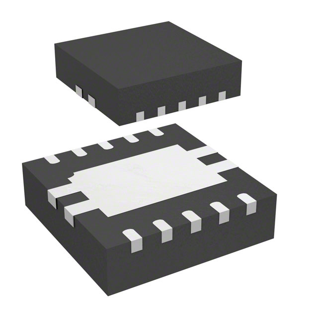
Device Package: TDFN 3x3-10L
Each channel of the PI5PD2560/2561 devices limit the
output current to a safe level by switching into a
constant-current mode when the output load exceeds the
current-limit threshold.
UL Listed – File No. E341484
The FAULTx logic output for each channel
independently asserts low during over-current or over
temperature.
CB Certified
Applications
USB Ports/Hubs
Digital TV
Set-Top Boxes
VOIP Phones
Typical Application Circuit
VIN
Pin Configuration
GND
1
IN
IN
EN1
EN2
2
IN
10 /FAULT1
9 OUT1
R2
100k
100k
C4
IN
C1
O UT2
C2
0.1uF
C3
/FAU LT1
IL IM
8 OUT2
7 ILIM
3
4
5
R1
O UT1
/FAU LT2
Logic signal
6 /FAULT2
R3
E N1
G ND
E N2
P ow er Pad
TDFN3.0x3.0-10L(Top View)
Pin Description
Pin No.
Pin Name
PI5PD2560
1
2, 3
4
/EN1
5
/EN2
Type
Description
PI5PD2561
GND
IN
EN1
I
I
Ground.
Power input voltage.
Enable input, logic low/high turns on channel one power switch.
EN2
I
Enable input, logic low/high turns on channel two power switch.
6
/FAULT2
O
7
ILIM
I
8
9
OUT2
OUT1
O
O
10
/FAULT1
O
Active-low open-drain output, asserted during over-current or
over-temperature condition occur on channel 2
External resistor used to set current-limit threshold; recommended
20 kΩ ≤ RILIM ≤ 187 kΩ.
Power switch output for channel two
Power switch output for channel one
Active-low open-drain output, asserted during over-current or
over-temperature condition occur on channel 1
2016-03-0004
PT0489-5
1
04/29/16
�PI5PD2560/2561
Dual Channel,
Adjustable Current-Limited Power Switch
|||||||||||||||||||||||||||||||||||||||||||||||||||||||||||||||||||||||||||||||||||||||||||||||||||||||||||||||||||||||||||||||||||||||||||||||||||||||||||||||||||||||||||||||||||||||||||||||||||||||||||||||||||||||||||||||||||||||||||||||||||||||||||||||||||||||||||||||||||||||||||||||||||||||||||||||||||||||||||||||||||||||
Maximum Ratings
Storage Temperature ................................................................................... -65oC to +150oC
Supply Voltage to Ground Potential ............................................................-0.5V to +6.0V
DC Input Voltage......................................................................................-0.5V to VDD+0.5V
Voltage range from IN to OUTx....................................................................-0.5V to+6.0V
Control Input Voltage (VINx).........................................................................-0.5V to+6.0V
Continuous total power dissipation(1).......................................................................2400mW
Continuous FAULTx sink current................................................................................25mA
Power Dissipation .............................................................................................................. 0.5W
ESD: HBM Mode...........................................................................................................4000V
CDM Mode.............................................................................................................. 500V
ESD-system level (contact/air)...............................................................................8kV/15kV
Note:
1. Stresses greater than those listed under
MAXIMUM RATINGS may cause permanent
damage to the device. This is a stress rating only
and functional operation of the device at these or
any other conditions above those indicated in the
operational sections of this specification is not
implied. Exposure to absolute maximum rating
conditions for extended periods may affect
reliability.
2. The JEDEC high-K (2s2p) board used to derive
this data was a 3in × 3in, multilayer board with 1ounce internal power and ground planes and 2ounce copper traces on top and bottom of the board.
Recommended operation conditions
Symbol
VIN
Parameter
Conditions
Min
Typ
Max
Unit
-
2.5
-
5.5
V
PI5PD2560
-
0
-
5.5
PI5PD2561
-
0
-
5.5
Input Voltage
VENx
Input Voltage
V/ENx
V
VIH
High-level input voltage on ENx
-
1.1
-
-
V
VIL
Low-level input voltage on ENx
-
-
-
0.66
V
IOUTx
Continuous output current per channel, OUTx
-
0
-
2.5
A
IFAULTx
Continuous /FAULTx sink current
-
-
-
10
mA
RILIM
Recommended resistor limit range
-
20
-
187
kΩ
Operating Temperature Range
-
-40
-
85
ºC
TA
2016-03-0004
PT0489-5
2
04/29/16
�PI5PD2560/2561
Dual Channel,
Adjustable Current-Limited Power Switch
|||||||||||||||||||||||||||||||||||||||||||||||||||||||||||||||||||||||||||||||||||||||||||||||||||||||||||||||||||||||||||||||||||||||||||||||||||||||||||||||||||||||||||||||||||||||||||||||||||||||||||||||||||||||||||||||||||||||||||||||||||||||||||||||||||||||||||||||||||||||||||||||||||||||||||||||||||||||||||||||||||||||
DC Electrical Characteristics
VI(IN)= 5.0V; TA=-40°C to +85°C; unless otherwise specified.
Sym
Test Conditions(1)
Description
Min
Typ
Max
Unit
mΩ
Power Switch
RDS(on)
Static drain-source on-state resistance
tr
Rise time, output
tf
Fall time, output
tIOS
Response time to short circuit
-
-
44
70
1
0.5
0.3
0.2
-
2
1
0.5
0.4
3.5
4
3
1.0
0.6
-
CL = 1F, RL = 100Ω
1.1
-
-
0.6
5
2
RILIM=20kΩ
RILIM=61.9kΩ
2590
800
2800
900
3005
1005
RILIM=100kΩ
400
560
645
2700
3160
3600
450
650
800
-
3.5
-
-
0.1
2
-
100
125
-
85
110
-
0.01
1.0
VIN Rising
-
2.35
2.45
V
TA=25°C
-
35
-
mV
I/FAULTx =1mA
-
-
180
mV
V/FAULTx =5.5V
FAULTx assertion or de-assertion
due to over-current condition
-
-
1
A
4
9
15
ms
VI(IN) = 5.0V
VI(IN) = 2.5V
VI(IN) = 5.0V
VI(IN) = 2.5V
VIN = 5.0 V
CL = 1F,
RL = 100Ω
-
ms
µs
Enable ENx
VIH
VIL
ton
toff
High-level input voltage
Low-level input voltage
Turn on time
Turn off time
2.5 V ≤ VI(IN) ≤ 5.5 V
2.5 V ≤ VI(IN) ≤ 5.5 V
V
ms
Current Limit
IOS
Current-limit threshold @ VOUTx = VIN * 0.8
VIN = 5 V, current ramp (≤ 100 A/s)
IOC_TRIP
tIOS
Overcurrent trip threshold
on OUT ,RILIM=20.0kΩ
VIN = 5 V, current ramp (≤ 100 A/s)
on OUT ,RILIM=100kΩ
Response time to short circuit
VIN = 5.0V
mA
s
Supply Current
ISTB
Input supply current at output disable
ISS
Input supply current at output enable
IREV
Reverse Leakage Current
No load on OUT, VEN=disable
TA =25°C
No load on OUT, RILIM=20kΩ
VEN=5.0V ,
RILIM=100kΩ
TA=25°C
VOUTx=5.5V, VIN=0V, TA=25°C
A
Under Voltage Lockout
UVLO
Low-level input voltage
Hysteresis for low-level input voltage
/FAULTx FLAG
VOL
Output low voltage
IOFF
Off-state leakage
TD
/FAULTx deglitch
Thermal Shutdown
OTSD2
OTSD
Thermal shutdown threshold
Thermal shutdown threshold in currentlimit
-
-
155
-
-
-
135
-
Hysteresis
-
-
20
-
°C
Note:
Pulse-testing techniques maintain junction temperature close to ambient temperature; thermal effects must be taken into account
separately.
2016-03-0004
PT0489-5
3
04/29/16
�PI5PD2560/2561
Dual Channel,
Adjustable Current-Limited Power Switch
|||||||||||||||||||||||||||||||||||||||||||||||||||||||||||||||||||||||||||||||||||||||||||||||||||||||||||||||||||||||||||||||||||||||||||||||||||||||||||||||||||||||||||||||||||||||||||||||||||||||||||||||||||||||||||||||||||||||||||||||||||||||||||||||||||||||||||||||||||||||||||||||||||||||||||||||||||||||||||||||||||||||
PARAMETER MEASUREMENT INFORMATION
Figure1 Test Circuit and Voltage Waveforms
Figure2 Response Time to Short Circuit Waveform
TYPICAL CHARACTERISTICS
VIN
IN
R1
R2
100k
100k
C1
0.1uF
O UT1
Channel One Output
C3
IN
O UT2
Channel Two Output
C2
/FAULT1 Signal
/FAU LT1
/FAULT2 Signal
/FAU LT2
IL IM
Chennel One Control Input
E N1
Chennel Two Control Input
E N2
R3
G ND
P ow er Pad
Figure3. Typical Characteristics Reference Schematic
2016-03-0004
PT0489-5
4
04/29/16
�PI5PD2560/2561
Dual Channel,
Adjustable Current-Limited Power Switch
|||||||||||||||||||||||||||||||||||||||||||||||||||||||||||||||||||||||||||||||||||||||||||||||||||||||||||||||||||||||||||||||||||||||||||||||||||||||||||||||||||||||||||||||||||||||||||||||||||||||||||||||||||||||||||||||||||||||||||||||||||||||||||||||||||||||||||||||||||||||||||||||||||||||||||||||||||||||||||||||||||||||
TYPICAL CHARACTERISTICS (Continued)
Figure 4. UVLO – Under voltage Lockout – V
Figure 5. IIN – Supply Current, Output Disabled – nA
Figure 6. IIN – Supply Current, Output Enabled – µA
Figure 7. IIN – Supply Current, Output Enabled – µA
2016-03-0004
PT0489-5
5
04/29/16
�PI5PD2560/2561
Dual Channel,
Adjustable Current-Limited Power Switch
|||||||||||||||||||||||||||||||||||||||||||||||||||||||||||||||||||||||||||||||||||||||||||||||||||||||||||||||||||||||||||||||||||||||||||||||||||||||||||||||||||||||||||||||||||||||||||||||||||||||||||||||||||||||||||||||||||||||||||||||||||||||||||||||||||||||||||||||||||||||||||||||||||||||||||||||||||||||||||||||||||||||
TYPICAL CHARACTERISTICS (Continued)
Figure 8. MOSFET rDS(on) Vs. Junction
Temperature
2016-03-0004
PT0489-5
6
04/29/16
�PI5PD2560/2561
Dual Channel,
Adjustable Current-Limited Power Switch
|||||||||||||||||||||||||||||||||||||||||||||||||||||||||||||||||||||||||||||||||||||||||||||||||||||||||||||||||||||||||||||||||||||||||||||||||||||||||||||||||||||||||||||||||||||||||||||||||||||||||||||||||||||||||||||||||||||||||||||||||||||||||||||||||||||||||||||||||||||||||||||||||||||||||||||||||||||||||||||||||||||||
Functional Description
Block Diagram
Overview
The PI5PD2560/2561 are a dual-channel, current-limited power-distribution switch using N-channel MOSFETs for applications
where short circuits or heavy capacitive loads will be encountered. This device allows the user to program the current-limit
threshold between 250 mA and 2.8 A (typ) per channel via an external resistor. This device incorporates an internal charge pump
and gate drive circuitry necessary to drive the N-channel MOSFETs. The charge pump supplies power to the driver circuit for
each channel and provides the necessary voltage to pull the gate of the MOSFET above the source. The charge pump operates
from input voltages as low as 2.5 V and requires little supply current. The driver controls the gate voltage of the power switch. The
driver incorporates circuitry that controls the rise and fall times of the output voltage to limit large current and voltage surges and
provides built-in soft-start functionality. Each channel of the PI5PD2560/2561 limit the output current to the programmed currentlimit threshold IOS during an over-current or short-circuit event by reducing the charge pump voltage driving the N-channel
MOSFET and operating it in the linear range of operation. The result of limiting the output current to I OS reduces the output
voltage at OUTx because the N-channel MOSFET is no longer fully enhanced.
Over-current Conditions
When an over-current condition is detected, the device maintains a constant output current and reduces the output voltage
accordingly.
The PI5PD2560/2561 thermal cycles if an overload condition is present long enough to activate thermal limiting in any of the
above cases. The device turns off when the junction temperature exceeds 135°C (min) while in current limit. The device remains
off until the junction temperature cools 20°C (typ) and then restarts. The PI5PD2560/2561 cycles on/off until the overload is
removed.
/FAULTx Response
The /FAULTx open-drain outputs are asserted (active low) on an individual channel during an over-current or Over temperature
condition. The PI5PD2560/2561 assert the FAULTx signal until the fault condition is removed and the device resumes normal
operation on that channel. The PI5PD2560/2561 are designed to eliminate false FAULTx reporting by using an internal delay
"deglitch" circuit (9-ms typ) for over-current conditions without the need for external circuitry. This ensures that FAULTx is not
accidentally asserted due to normal operation such as starting into a heavy capacitive load. The deglitch circuitry delays entering
and leaving current-limited induced fault conditions. The FAULTx signal is not deglitched when the MOSFET is disabled due to
an over temperature condition but is deglitched after the device has cooled and begins to turn on. This unidrectional deglitch
prevents FAULTx oscillation during an overt temperature event.
2016-03-0004
PT0489-5
7
04/29/16
�PI5PD2560/2561
Dual Channel,
Adjustable Current-Limited Power Switch
|||||||||||||||||||||||||||||||||||||||||||||||||||||||||||||||||||||||||||||||||||||||||||||||||||||||||||||||||||||||||||||||||||||||||||||||||||||||||||||||||||||||||||||||||||||||||||||||||||||||||||||||||||||||||||||||||||||||||||||||||||||||||||||||||||||||||||||||||||||||||||||||||||||||||||||||||||||||||||||||||||||||
Under-voltage Lockout (UVLO)
The under-voltage lockout (UVLO) circuit disables the power switch until the input voltage reaches the UVLO turn-on threshold.
Built-in hysteresis prevents unwanted on/off cycling due to input voltage droop during turn on.
Enable (ENx OR /ENx)
The logic enables control the power switches and device supply current. The supply current is reduced to less than 2μA when a
logic high is present on /ENx or when a logic low is present on ENx. A logic low input on /ENx or a logic high input on ENx
enables the driver, control circuits, and power switches. The enable inputs are compatible with both TTL and CMOS logic levels.
Thermal Sense
The PI5PD2560/2561 self protect by using two independent thermal sensing circuits that monitor the operating temperature of the
power switch and disable operation if the temperature exceeds recommended operating conditions. Each channel of the
PI5PD2560/2561 operate in constant-current mode during over-current conditions, which increases the voltage drop across the
power switch. The power dissipation in the package is proportional to the voltage drop across the power switch, which increases
the junction temperature during an over-current condition. The first thermal sensor (OTSD) turns off the individual power switch
channel when the die temperature exceeds 135°C (min) and the channel is in current limit. Hysteresis is built into the thermal
sensor, and the switch turns on after the device has cooled approximately 20°C.
The PI5PD2560/2561 also have a second ambient thermal sensor (OTSD2). The ambient thermal sensor turns off both power
switch channels when the die temperature exceeds 155°C (min) regardless of whether the power switch channels are in current
limit and will turn on the power switches after the device has cooled approximately 20°C. The PI5PD2560/2561 continue to cycle
off and on until the fault is removed.
APPLICATION INFORMATION
INPUT AND OUTPUT CAPACITANCE
Input and output capacitance improves the performance of the device; the actual capacitance should be optimized for the particular
application. For all applications, a 0.1μF or greater ceramic bypass capacitor between IN and GND is recommended as close to the
device as possible for local noise decoupling. This precaution reduces ringing on the input due to power-supply transients.
Additional larger input capacitance with low ESR is needed on the input to reduce voltage overshoot from exceeding the absolute
maximum voltage of the device during heavy transient conditions. This is especially important during bench testing when long,
inductive cables are used to connect the evaluation board to the bench power supply.
Output capacitance is not required, but placing a high-value electrolytic capacitor on the output pin is recommended when large
transient currents are expected on the output.
PROGRAMMING THE CURRENT-LIMIT THRESHOLD
The over-current threshold is user programmable via an external resistor, RILIM. RILIM sets the current-limit threshold for both
channels. The PI5PD2560/2561 use an internal regulation loop to provide a regulated voltage on the ILIM pin. The current-limit
threshold is proportional to the current sourced out of ILIM. The recommended 1% resistor range for RILIM is 20 kΩ ≤ RILIM ≤
187 kΩ to ensure stability of the internal regulation loop. Many applications require that the minimum current limit is above a
certain current level or that the maximum current limit is below a certain current level, so it is important to consider the tolerance
of the over-current threshold when selecting a value for RILIM. The following equations calculates the resulting overcurrent
threshold for a given external resistor value (RILIM). The traces routing the RILIM resistor to the PI5PD2560/2561 should be as
short as possible to reduce parasitic effects on the current-limit accuracy.
IOSmax (mA) =
52850V
RILIM0.957kΩ
IOSnom (mA) =
56000V
RILIMkΩ
IOSmin (mA) =
61200V
RILIM1.056kΩ
2016-03-0004
PT0489-5
8
04/29/16
�PI5PD2560/2561
Dual Channel,
Adjustable Current-Limited Power Switch
|||||||||||||||||||||||||||||||||||||||||||||||||||||||||||||||||||||||||||||||||||||||||||||||||||||||||||||||||||||||||||||||||||||||||||||||||||||||||||||||||||||||||||||||||||||||||||||||||||||||||||||||||||||||||||||||||||||||||||||||||||||||||||||||||||||||||||||||||||||||||||||||||||||||||||||||||||||||||||||||||||||||
(2)
Figure 9. Current-Limit Threshold vs. RILIM
APPLICATION 1: DESIGNING ABOVE A MINIMUM CURRENT LIMIT
Some applications require that current limiting cannot occur below a certain threshold. For this example, assume that 2 A must be
delivered to the load so that the minimum desired current-limit threshold is 2000 mA. Use the IOS equations and Figure 9 to
select RILIM.
IOSmax (mA) = 2000mA
IOSmin (mA) =
61200V
RILIM1.056kΩ
RILIM (kΩ) =
61200V
IOsmin mA
1
1.056
RILIM (kΩ) = 25.52kΩ
Select the closest 1% resistor less than the calculated value: RILIM = 25.5 kΩ. This sets the minimum current-limit threshold at
2A. Use the IOS equations, Figure 9, and the previously calculated value for RILIM to calculate the maximum resulting currentlimit threshold
RILIM (kΩ) = 25.52kΩ
IOSmax (mA) =
IOSmax (mA) =
52850V
RILIM0.957kΩ
52850V
25.50.957kΩ
IOSmax (mA) = 2382mA
The resulting maximum current-limit threshold is 2382 mA with a 25.5 kΩ resistor
2016-03-0004
PT0489-5
9
04/29/16
�PI5PD2560/2561
Dual Channel,
Adjustable Current-Limited Power Switch
|||||||||||||||||||||||||||||||||||||||||||||||||||||||||||||||||||||||||||||||||||||||||||||||||||||||||||||||||||||||||||||||||||||||||||||||||||||||||||||||||||||||||||||||||||||||||||||||||||||||||||||||||||||||||||||||||||||||||||||||||||||||||||||||||||||||||||||||||||||||||||||||||||||||||||||||||||||||||||||||||||||||
APPLICATION 2: DESIGNING BELOW A MAXIMUM CURRENT LIMIT
Some applications require that current limiting must occur below a certain threshold. For this example, assume that the desired
upper current-limit threshold must be below 1000 mA to protect an up-stream power supply. Use the IOS equations and Figure 9
to select RILIM.
IOSmax (mA) = 1000mA
IOSmax (mA) =
RILIM (kΩ) =
52850V
RILIM0.957kΩ
1
0.957
52850V
IOsmaxmA
RILIM (kΩ) = 63.16kΩ
Select the closest 1% resistor greater than the calculated value: RILIM = 63.4 kΩ. This sets the maximum current-limit threshold
at 1000 mA. Use the IOS equations, Figure 9, and the previously calculated value for RILIM to calculate the minimum resulting
current-limit threshold
RILIM (kΩ) = 63.4kΩ
IOSmin (mA) =
61200V
RILIM1.056kΩ
IOSmin (mA) =
61200V
63.41.056kΩ
IOSmin (mA) = 765mA
The resulting minimum current-limit threshold is 765 mA with a 63.4 kΩ resistor.
ACCOUNTING FOR RESISTOR TOLERANCE
The previous sections described the selection of R ILIM given certain application requirements and the importance of understanding
the current-limit threshold tolerance. The analysis focused only on the PI5PD2560A/2561A performance and assumed an exact
resistor value. However, resistors sold in quantity are not exact and are bounded by an upper and lower tolerance centered around
a nominal resistance. The additional RILIM resistance tolerance directly affects the current-limit threshold accuracy at a system
level. The following table shows a process that accounts for worst-case resistor tolerance assuming 1% resistor values. Step one
follows the selection process outlined in the application examples above. Step two determines the upper and lower resistance
bounds of the selected resistor. Step three uses the upper and lower resistor bounds in the IOS equations to calculate the threshold
limits. It is important to use tighter tolerance resistors, e.g. 0.5% or 0.1%, when precision current limiting is desired.
Desired Nominal
Current Limit
(mA)
Ideal
Resistor
(kΩ)
Closest 1%
Resistor
(kΩ)
300
400
600
800
1000
1200
1400
1600
1800
2000
2200
2400
2600
2800
186.7
140
93.3
70
56
46.7
40
35
31.1
28
25.5
23.3
21.5
20
187
140
93.1
69.8
56.2
46.4
40.2
34.8
30.9
28
25.5
23.2
21.5
20
Resistor Tolerance
1% low
(kΩ)
185.1
138.6
92.2
69.1
55.6
45.9
39.8
34.5
30.6
27.7
25.2
23
21.3
19.8
2016-03-0004
1%
high(kΩ)
188.9
141.4
94
70.5
56.8
46.9
40.6
35.1
31.2
28.3
25.8
23.4
21.7
20.2
Actual Limits
IOS MIN
(mA)
241.6
328
504.6
684
859.9
1052.8
1225
1426.5
1617.3
1794.7
1981
2188.9
2372.1
2560.4
IOS Nom
(mA)
299.5
400
601.5
802.3
996.4
1206.9
1393
1609.2
1812.3
2000
2196.1
2413.8
2604.7
2800
IOS MAX
(mA)
357.3
471.4
696.5
917.6
1129.1
1356.3
1555.9
1786.2
2001.4
2199.3
2405.3
2633
2831.9
3034.8
PT0489-5
10
04/29/16
�PI5PD2560/2561
Dual Channel,
Adjustable Current-Limited Power Switch
|||||||||||||||||||||||||||||||||||||||||||||||||||||||||||||||||||||||||||||||||||||||||||||||||||||||||||||||||||||||||||||||||||||||||||||||||||||||||||||||||||||||||||||||||||||||||||||||||||||||||||||||||||||||||||||||||||||||||||||||||||||||||||||||||||||||||||||||||||||||||||||||||||||||||||||||||||||||||||||||||||||||
AUTO-RETRY FUNCTIONALITY
Some applications require that an overcurrent condition disables the part momentarily during a fault condition and re-enables after
a pre-set time. This auto-retry functionality can be implemented with an external resistor and capacitor. During a fault condition,
FAULTx pulls ENx low disabling the part. The part is disabled when ENx is pulled below the turn-off threshold, and FAULTx
goes high impedance allowing CRETRY to begin charging. The part re-enables when the voltage on ENx reaches the turn-on
threshold, and the auto-retry time is determined by the resistor/capacitor time constant. The part will continue to cycle in this
manner until the fault condition is removed.
VIN
IN
R1
R2
100k
100k
C1
0.1uF
O UT1
VOU T1
C3
IN
O UT2
VOU T2
C2
/FAU LT1
IL IM
E N1
C2
0.22uF
R3
20k
/FAU LT2
G ND
E N2
P ow er Pad
C3
0.22uF
Figure 10.Auto-Retry Functionality
Some applications require auto-retry functionality and the ability to enable/disable with an external logic signal. The figure below
shows how an external logic signal can drive EN through RFAULT and maintain auto-retry functionality. The resistor/capacitor
time constant determines the auto-retry time-out period.
VIN
IN
C1
0.1uF
Logic signal & drivers
O UT1
VOU T1
C3
IN
O UT2
VOU T2
C2
R1
/FAU LT1
100k
IL IM
E N1
R3
20k
R2
/FAU LT2
100k
G ND
E N2
C2
0.22uF
P ow er Pad
C3
0.22uF
Figure 11.Auto-Retry Functionality With External EN Signal
2016-03-0004
PT0489-5
11
04/29/16
�PI5PD2560/2561
Dual Channel,
Adjustable Current-Limited Power Switch
|||||||||||||||||||||||||||||||||||||||||||||||||||||||||||||||||||||||||||||||||||||||||||||||||||||||||||||||||||||||||||||||||||||||||||||||||||||||||||||||||||||||||||||||||||||||||||||||||||||||||||||||||||||||||||||||||||||||||||||||||||||||||||||||||||||||||||||||||||||||||||||||||||||||||||||||||||||||||||||||||||||||
Mechanical Information
TDFN 3.0x3.0-10L
Ordering Information
Part No.
Package Code
Package
PI5PD2560ZEEX
ZE
Lead free and Green 10-pin TDFN3.0x3.0
PI5PD2561ZEEX
ZE
Lead free and Green 10-pin TDFN3.0x3.0
Tape & reel
Tape & reel
Note:
E = Pb-free and Green
Adding X Suffix= Tape/Reel
Pericom Semiconductor Corporation 1-800-435-2336 www.pericom.com
Pericom reserves the right to make changes to its products or specifications at any time, without notice, in order to improve design or performance and to supply
the best possible product. Pericom does not assume any responsibility for use of any circuitry described other than the circuitry embodied in Pericom product. The
company makes no representations that circuitry described herein is free from patent infringement or other rights, of Pericom.
2016-03-0004
PT0489-5
12
04/29/16
�


 工商网监
湘ICP备2023018690号
工商网监
湘ICP备2023018690号
