PI6C18551
3.3V/5V, 160 MHz,
4 output, CMOS Clock Buffer
Features
Description
•
•
•
•
•
•
•
PI6C18551 is a low skew, low noise and high-speed clock buffer
for computing, networking and communication applications. It is
a non-inverting buffer with four outputs from a single input. The
outputs are controlled by output enable pin (OE), outputs are tri-states
when OE is LOW, and outputs are enabled when OE is HIGH.
160 MHz maximum frequency
Low skew: 250ps
Fast rise/fall time: 1.5ns
Output Enable with tri-states
Industrial Temperature
3.3V or 5V power supply
Packaging (Pb-free & Green available):
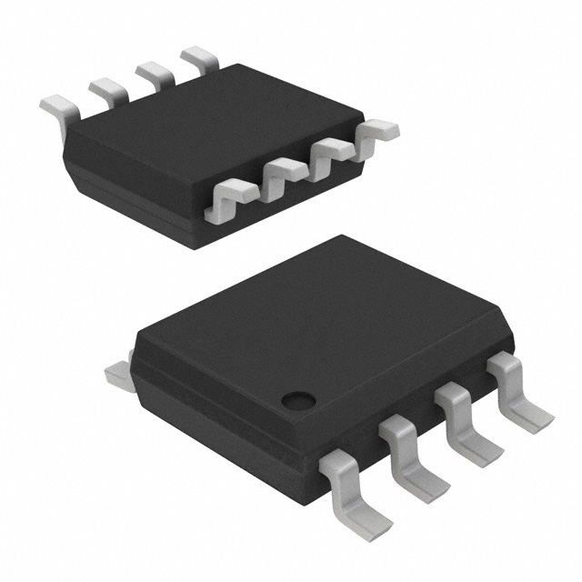
−8-pin SOIC (W)
Pin Description
Applications
•
•
•
•
•
33 MHz for PCI
106.25 MHz for Fibre Channel
125 MHz for Ethernet
133 MHz for PCIX
155.52 MHz for OC3/SONET
CLK_IN
1
8
OE*
Y0
2
7
VDD
Y1
3
6
GND
Y2
4
5
Y3
*External pull-up recommended
Logic Block Diagram
Y0
Function Table
Inputs
Y1
Y2
CLK_IN
Y3
OE
10-0157
Outputs
CLK_IN
OE
Y[3:0]
X
L
Z
L
H
L
H
H
H
Note:
1. X = Don't Care; Z = Tri-state
1
PS8733E
04/20/10
�PI6C18551
3.3V/5V, 160 MHz,
4 output, CMOS Clock Buffer
Pin Description
Pin Name
Type
Pin No
Descriptions
CLK_IN
Input
1
Input clock with pull-up resistor
Y0
Output
2
Output clock
Y1
Output
3
Output clock
Y2
Output
4
Output clock
Y3
Output
5
Output clock
GND
Ground
6
GROUND
VDD
Power
7
3.3V or 5V power supply
OE
Input
8
Output Enable with pull-up resistor. External
pull-up resistor is recommended.
External Components
A minimum number of external components are required for proper operation. A decoupling capacitor of 0.01μF should be connected
between VDD on pin 7 and GND on pin 6, as close to the device as possible. A 33-Ohm series terminating resistor may be used on
each clock output if the trace is longer than 1 inch. An external 100k-Ohm pull-up resistor should be used on pin 8, OE.
Absolute Maximun Ratings (Over operating free-air temperature range)
Symbol
VDD
Parameters
Min.
Supply Voltage
Max.
Units
7
VI
Input Voltage
-0.5
VDD+0.5
VO
Output Voltage
-0.5
VDD+0.5
Ts
Storage Temperature
-65
150
Ta
Ambient Temperature
-40
85
Tso
Soldering Temperature
10-0157
V
°C
260
2
PS8733E
04/20/10
�PI6C18551
3.3V/5V, 160 MHz,
4 output, CMOS Clock Buffer
DC Electrical Characteristics (VDD = 3.3V ±5%, TA = -40 to 85°C)
Symbol
Parameters
Condition
VDD
3.3V I/O Supply Voltage
VIH
Input High Voltage
VIL
Input Low Voltage
VOH
Output High Voltage
IOH = -12mA
VOL
Output Low Voltage
IOL = 12mA
IDD
Power Supply Current
ZO
Output Impedance
RPU
Internal Pull-up Resistor
IOS
Short Circuit Current
Min.
Typ.
Max.
3.135
3.465
CLK_IN, Note 1
VDD/2 + 0.7
3.8
OE
2
VDD
CLK_IN, Note 1
VDD/2 - 0.7
OE
0.8
No load at 135 MHz
CLK_IN & OE
Units
V
2.4
0.4
34
mA
20
Ohm
192
kOhm
−46
mA
Notes:
1. Nominal switching threshold is VDD/2
10-0157
3
PS8733E
04/20/10
�PI6C18551
3.3V/5V, 160 MHz,
4 output, CMOS Clock Buffer
DC Electrical Characteristics (VDD = 5V ±5%, TA = -40 to 85°C)
Symbol
Parameters
VDD
5V I/O Supply Voltage
VIH
Input High Voltage
VIL
Input Low Voltage
VOL
Condition
Min.
Typ.
Max.
4.75
5.25
CLK_IN, Note 1
VDD/2 + 1
5.5
OE
2
VDD
CLK_IN, Note 1
VDD/2 - 1
OE
0.8
Output Low Voltage
IOL = 12mA
0.4
VOH
Output High Voltage
(CMOS Level)
IOH = -12mA
IDD
Power Supply Current
No load at 135MHz
ZO
Output Impedance
RPU
Internal Pull-up Resistor
IOS
Short Circuit Current
Units
V
4
CLK_IN & OE
61
mA
20
Ohm
193
k-Ohm
−90
mA
Notes:
1. Nominal switching threshold is VDD/2
AC Electrical Characteristics (VDD = 3.3±5%, TA = -40 to 85°C)
Symbol
Parameters
Fin
Input Frequency
Fo
Output Frequency
Condition
Min.
Typ.
0
160
load(5)
Fo
Output Frequency
TR
Rise Time
0.8V to 2.0V
1.5
TF
Fall Time
2.0V to 0.8V
1.5
TPD
Propagation Delay
TPD
Propagation Delay
TSK
Output Skew
Tjit
Additive Jitter
3.3V,
135MHz(2)
5V, 135MHz(2)
VDD
MHz
135
2
4
8
1.5
3
6
/2(3)
RMS @ 12KHz~20MHz
Units
160
3.3V, 15pF load(5)
5V, l5pF
Max.
250
45.6
ns
ps
fs
Notes:
1. With rail to rail input clock.
2. All outputs with equal loading.
3. Duty cycle on outputs will match incoming clock duty cycle.
4. With external series resistor 33Ω positioned close to each output pin.
10-0157
4
PS8733E
04/20/10
�PI6C18551
3.3V/5V, 160 MHz,
4 output, CMOS Clock Buffer
Jitter (RMS @ 12KHz~20MHz)
Output phase noise vs. input (light
blue line) plot
Output RMS phase jitter=156.4fs
Input phase noise plot
Input RMS phase jitter=149.6fs
10-0157
5
PS8733E
04/20/10
�PI6C18551
3.3V/5V, 160 MHz,
4 output, CMOS Clock Buffer
Packaging Mechcanical: 8-pin SOIC (W)
DOCUMENT CONTROL NO.
8
PD - 1001
REVISION: F
.149
.157
DATE: 03/09/05
3.78
3.99
.0099
.0196
0.25
x 45˚
0.50
1
.189
.196
4.80
5.00
.0075
.0098
0-8˚
0.19
0.25
0.40 .016
1.27 .050
1
.016
.026
0.406
0.660
.2284
.2440
5.80
6.20
.053 1.35
.068 1.75
SEATING PLANE
REF
.050
BSC
1.27
.0040 0.10
.0098 0.25
.013 0.330
.020 0.508
Pericom Semiconductor Corporation
3545 N. 1st Street, San Jose, CA 95134
1-800-435-2335 • www.pericom.com
X.XX DENOTES DIMENSIONS
X.XX IN MILLIMETERS
Notes:
1) Controlling dimensions in millimeters.
2) Ref: JEDEC MS-012D/AA
DESCRIPTION: 8-Pin, 150-Mil Wide, SOIC
PACKAGE CODE: W
Ordering Information(1,2,3):
Ordering Code
PI6C18551WE
Package Code
Package Description
W
Pb-free & Green, 8-pin SOIC
Notes:
1. Thermal characteristics can be found on the company web site at www.pericom.com/packaging/
2. E = Pb-free and Green
3. Adding an X Suffix = Tape/Reel
Pericom Semiconductor Corporation • 1-800-435-2336 • www.pericom.com
10-0157
6
PS8733E
04/20/10
�
很抱歉,暂时无法提供与“PI6C18551WEX”相匹配的价格&库存,您可以联系我们找货
免费人工找货