PI6C2409-1H
Zero-Delay Clock Buffer
Features
Description
•
•
•
•
The PI6C2409-1H is a PLL based, zero-delay buffer, with the ability
to distribute nine outputs of up to 133 MHz at 3.3V.
All the outputs are distributed from a single clock input CLKIN and
output OUT0 performs zero delay by connecting a feedback to PLL.
•
•
•
Maximum rated frequency: 133 MHz
Low cycle-to-cycle jitter
Input to output delay, less than 200ps
Internal feedback allows outputs to be synchronized to the
clock input
Spread spectrum compatible
Operates at 3.3V VDD
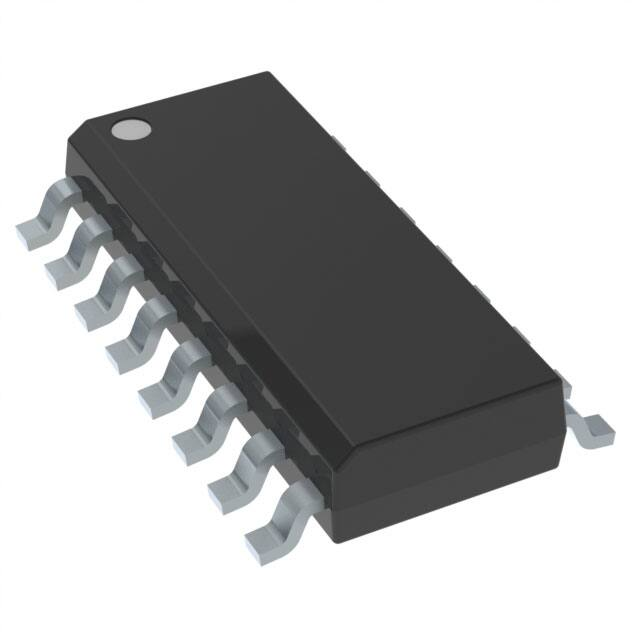
Space-saving Package: (Pb-free & Green available)
- 16-Pin TSSOP (L)
- 16-Pin SOIC (W)
PI6C2409-1H has two banks of four outputs that can be controlled by
the selection inputs, SEL1 & SEL2. It also has a power sparing feature:
when input SEL1 is 0 and SEL2 is 1, PLL is turned off and all
outputs are referenced from CLKIN. PI6C2409-1H is available in
high drive and industrial environment versions.
An internal feedback on OUT0 is used to synchronize the
outputs to the input; the relationship between loading of this signal
and the outputs determines the input-output delay.
PI6C2409-1H are characterized for both commercial and
industrial operation
Block Diagram
Pin Configuration
PLL
CLKIN
CLKIN
OUTA1
OUTA2
VDD
GND
OUTB1
OUTB2
SEL2
OUT0
MUX
OUTA1
OUTA2
OUTA3
SEL1
SEL2
Decode
Logic
OUTA4
OUTB1
OUTB2
PI6C2409-1H
All trademarks are property of their respective owners.
OUTB3
OUTB4
15-0174
1
16
1
15
2
14
3
4 16-Pin 13
5 W, L 12
11
6
10
7
9
8
OUT0
OUTA4
OUTA3
VDD
GND
OUTB4
OUTB3
SEL1
www.pericom.com 12/02/15
�PI6C2409-1H
Zero-Delay Clock Buffer
Input Select Decoding
SEL2
SEL1
OUTA [1-4]
OUTB [1-4]
0
0
1
1
0
1
0
1
3-State
PLL
CLKIN
PLL
3-State
3-State
CLKIN
PLL
Output Source
(OUT0)
PLL
PLL
CLKIN
PLL
PLL
ON
ON
OFF
ON
Pin Description
Pin
Signal
Description
1
2, 3, 14, 15
4, 13
5, 12
6, 7, 10 ,11
8
9
16
CLKIN
OUTA[1-4]
VDD
GND
OUTB[1-4]
SEL2
SEL1
OUT0
Input clock reference frequency (weak pull-down)
Clock outputs, Bank A
3.3V supply
Ground
Clock outputs, Bank B
Select input, bit 2 (weak pull-up)
Select input, bit 1 (weak pull-up)
Clock Output , internal PLL feedback
Zero-Delay and Skew Control
CLKIN Input to OUTx Delay vs. Difference in Loading between OUT0 pin and OUTx pins
CLKIN - Input to OUTx Delay (ps)
800
600
400
200
0
-200
-25
-20
-15
-10
0
-5
5
10
15
-400
20
25
PI6C2409-1H
-600
-800
-900
-1000
Output Load Difference: OUT0 Load - OUTx Load (pF)
The relationship between loading of the OUT0 signal and other outputs determines the input-output delay. Zero delay is achieved when
all outputs, including feedback, are loaded equally.
All trademarks are property of their respective owners.
15-0174
2
www.pericom.com
11/21/ 2015
�PI6C2409-1H
Zero-Delay Clock Buffer
Maximum Ratings
(Above which useful life may be impaired. For user guidelines, not tested.)
Storage Temperature........................................................... –65°C to +150°C
Supply Voltage to Ground Potential....................................–0.5V to +4.6V
DC Input Voltage......................................................... –0.5V to VDD +0.5V
ESD Protection (Input).................................................. 2000 V min (HBM)
Note: Stresses greater than those listed under MAXIMUM RATINGS may cause permanent damage to the
device. This is a stress rating only and functional operation of the device at these or any other conditions
above those indicated in the operational sections of
this specification is not implied. Exposure to absolute
maximum rating conditions for extended periods may
affect reliability.
Operating Conditions (VCC = 3.3V ±0.3V)
Parameter
VDD
TA
CL
CIN
Description
Supply Voltage
Commercial Operating Temperature
Industrial Operating Temperature
Load Capacitance, below 100 MHz
Load Capacitance, from 100 MHz to 133 MHz
Input Capacitance
Min.
Max.
Units
3.0
0
-40
3.6
70
85
30
15
7
V
-
ºC
pF
DC Electrical Characteristics for Industrial Temperature Devices
Parameters
VIL
VIH
IIL
IIH
VOL
VOH
IDD
Description
Input LOW Voltage
Input HIGH Voltage
Input LOW Current
Input HIGH Current
Output LOW Voltage
Output HIGH Voltage
Bypass, PLL OFF
Supply Current
All trademarks are property of their respective owners.
Test Conditions
Min.
Max.
0.8
2.0
VIN = 0V
VIN = VDD
IOL = 12mA
IOH = –12mA
SEL1 = 0, SEL2 = 1
Unloaded outputs 100 MHz, Select inputs at
VDD or GND
Unloaded outputs 66 MHz, CLKIN
15-0174
3
50.0
125
0.4
2.4
Units
V
µA
V
1.0
62
mA
44
www.pericom.com
11/21/ 2015
�PI6C2409-1H
Zero-Delay Clock Buffer
AC Electrical Characteristics for Industrial Temperature Devices
Parameters
Name
FO
Output Frequency
Duty Cycle(1)
tDC
tR
tF
tSK(O)
t0
Duty
Cycle(1)
Rise Time(1)
Fall Time(1)
Output to Output Skew(1)
Delay, CLKIN Rising Edge
to OUT0 Rising Edge(1)
tSK(D)
Device-to-Device Skew(1)
tSLEW
Output Slew Rate(1)
tJIT
Cycle-to-Cycle Jitter(1)
tLOCK
PLL Lock Time(1)
Test Conditions
30pF load
10pF load
Measured at VDD/2,
FOUT = 66.67 MHz
Measured at VDD/2V,
FOUT
很抱歉,暂时无法提供与“PI6C2409-1HWIE”相匹配的价格&库存,您可以联系我们找货
免费人工找货