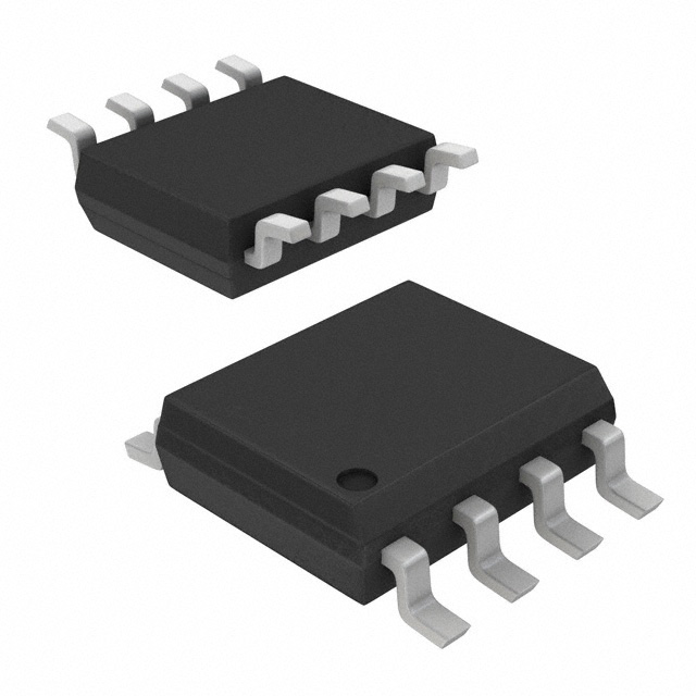
PI6C2501
12345678901234567890123456789012123456789012345678901234567890121234567890123456789012345678901212345678901234567890123456789012123456789012
12345678901234567890123456789012123456789012345678901234567890121234567890123456789012345678901212345678901234567890123456789012123456789012
Phase-Locked Loop Clock Driver
Product Features
Product Description
• High-Performance, Phase-Locked-Loop Clock Distribution
The PI6C2501 features a low-skew, low-jitter, phase-locked loop
(PLL) clock driver. By connecting the CLK_OUT output to the
feedback FB_IN input, the propagation delay from the CLK_IN
input to CLK_OUT output will be nearly zero.
• Allows Clock Input to have Spread Spectrum modulation
for EMI reduction
• Zero Input-to-Output delay
• Low jitter: Cycle-to-Cycle jitter ±100ps max.
Application
• On-chip series damping resistor at clock output drivers
for low noise and EMI reduction
If a system designer needs more than 16 outputs with the features
just described, using two or more zero-delay buffers, such as the
PI6C2509Q, or PI6C2510Q, is likely to be impractical. The
device-to-device skew introduced can significantly reduce the
performance. Pericom recommends using a zero-delay buffer and
an eighteen output non-zero-delay buffer. As shown in Figure 1,
this combination produces a zero-delay buffer with all the signal
characteristics of the original zero-delay buffer, but with as many
outputs as the non-zero-delay buffer part. For example, when
combined with an eighteen output non-zero delay buffer, a system
designer can create a seventeen-output zero-delay buffer.
• Operates at 3.3V VCC
• Wide range of Clock Frequencies up to 80 MHz
• Package: Plastic 8-pin SOIC (W)
Product Pin Configuration
Logic Block Diagram
FB_IN
AGND
GND
CLK_OUT
AVCC
VCC
CLK_IN
CLK_OUT
PLL
1
2
3
4
8-Pin
W
8
7
6
5
CLK_IN
AVCC
GND
FB_IN
Feedback
Reference
Clock
Signal
Zero Delay
Buffer
PI6C2501
CLK_OUT
18 Outputs
Non-PLL
Buffer
V
C
17
Figure 1. This Combination Provides Zero-Delay Between
the Reference Clock Signal and 17 Outputs
1
PS8381A
07/17/00
�PI6C2501
Phase-Locked
Loop
Clock
Driver
12345678901234567890123456789012123456789012345678901234567890121234567890123456789012345678901212345678901234567890123456789012123456789012
Pin Functions
Pin Name
Pin No.
Type
D e s cription
CLK _IN
8
I
Reference Clock input. CLK _IN allows spread spectrum clock input.
FB_IN
5
I
Feedback input. FB_IN provides the feedback signal to the internal PLL.
CLK _O UT
3
O
Clock output. This output provides a low- skew copy of CLK _IN. The output has an embedded
series- damping resistor.
AVC C
7
Power
Analog power supply. AVC C can be also used to bypass the PLL for test purpose. When AVC C
is strapped to ground, PLL is bypassed and CLK _IN is buffered directly to the device outputs.
AGND
1
Ground
Analog ground. AGND provides the ground reference for the analog circuitry.
VC C
4
Power
Power supply.
GND
2, 6
Ground
Ground.
DC Specifications (Absolute maximum ratings over operating free-air temperature range)
Symbol
Parame te r
VI
Input voltage range
VO
Output voltage range
M in.
M ax.
Units
- 0.5
VCC +0.5
V
IO_DC
DC output current
100
mA
Power
Maximum power dissipation at TA = 55oC in still air
1.0
W
TSTG
Storage temperature
150
oC
M ax.
Units
10
µA
65
Note:
Stress beyond those listed under absolute maximum ratings may cause permanent damage to the device.
Parame te r
Te s t Conditions
ICC
VI = VCC or GND; IO = 0(1)
CI
VI = VCC or GND
CO
VO =VCC or GND
VCC
M in.
Typ.
3.6V
4
3.3V
pF
6
Note:
1. Continuous Output Current
Recommended Operating Conditions
Symbol
Parame te r
M in.
M ax.
3.6
VCC
Supply voltage
3.0
VIH
High level input voltage
2.0
VIL
Low level input voltage
VI
Input voltage
0
VCC
TA
Operating free- air temperature
0
70
0.8
2
Units
V
ºC
PS8381A
07/17/00
�PI6C2501
Phase-Locked
Loop
Clock
Driver
12345678901234567890123456789012123456789012345678901234567890121234567890123456789012345678901212345678901234567890123456789012123456789012
Electrical Characteristics (Over Recommended Operating Free-Air Temperature Range
Pull Up/Down Currents of PI6C2501, VCC = 3.0V)
Symbol
IOH
IOL
Parame te r
Condition
M in.
M ax.
Pull- up current
Vout = 2.4V
- 18
Pull- up current
Vout = 2.0V
- 30
Pull- down current
Vout = 0.8V
25
Pull- down current
Vout = 0.55V
17
Units
mA
AC Specifications
(Timing requirements over recommended ranges of supply voltage and operating free-air temperature)
Symbol
Parame te r
M in.
M ax.
Units
FCLK
Clock frequency PI6C2501
25
80
MHz
DCYI
Input clock duty cycle
40
60
%
1
ms
Stabilization Time after power up
Switching Characteristics
(Over recommended ranges of supply voltage and operating free-air temperature, CL = 30pF)
Parame te r
From (Input)
tphase error without jitter
CLK_IN↑ at 100 & 66 MHz
Jitter, cycle- to- cycle
At 100 & 66 MHz
To (Output)
FB_IN↑
Duty cycle
CLK_OUT
tr, rise- time, 0.4V to 2.0V
tf, fall- time, 2.0V to 0.4V
VCC = 3.3V ±0.3V, 0-70°C
M in.
Typ.
M ax.
150
+150
100
+100
45
55
1.0
Units
ps
%
ns
1.1
Note:
These switching parameters are guaranteed by design.
3
PS8381A
07/17/00
�PI6C2501
Phase-Locked
Loop
Clock
Driver
12345678901234567890123456789012123456789012345678901234567890121234567890123456789012345678901212345678901234567890123456789012123456789012
Package Mechanical Information: Plastic 8-pin SOIC Package.
8
.149
.157
3.78
3.99
.0099
.0196
0.25
x 45˚
0.50
1
.189
.196
4.80
5.00
.0075
.0098
0-8˚
0.19
0.25
0.40 .016
1.27 .050
.016
.026
0.406
0.660
.2284
.2440
5.80
6.20
1.35
1.75
.053
.068
SEATING PLANE
REF
.050
BSC
1.27
.0040 0.10
.0098 0.25
.013 0.330
.020 0.508
X.XX DENOTES DIMENSIONS
X.XX IN MILLIMETERS
Ordering Information
Orde ring Code
Package Name
Package Type
Ope rating Range
PI6C2501W
W8
8- pin 150- mil SO IC
Commercial
Pericom Semiconductor Corporation
2380 Bering Drive • San Jose, CA 95131 • 1-800-435-2336 • Fax (408) 435-1100 • http://www.pericom.com
4
PS8381A
07/17/00
�
很抱歉,暂时无法提供与“PI6C2501WE”相匹配的价格&库存,您可以联系我们找货
免费人工找货