PI6C2502A
12345678901234567890123456789012123456789012345678901234567890121234567890123456789012345678901212345678901234567890123456789012123456789012
12345678901234567890123456789012123456789012345678901234567890121234567890123456789012345678901212345678901234567890123456789012123456789012
12345678901234567890123456789012123456789012345678901234567890121234567890123456789012345678901212345678901234567890123456789012123456789012
Phase-Locked Loop Clock Driver
Product Features
Product Description
• High-Performance Phase-Locked-Loop Clock Distribution
for Networking,
• Synchronous DRAM modules for server/workstation/
PC applications
• Allows Clock Input to have Spread Spectrum
modulation for EMI reduction
• Zero Input-to-Output delay
• Low jitter: Cycle-to-Cycle jitter ±75ps max.
• On-chip series damping resistor at clock output drivers
for low noise and EMI reduction
• Operates at 3.3V VCC
• Wide range of Clock Frequencies 80 to 134 MHz
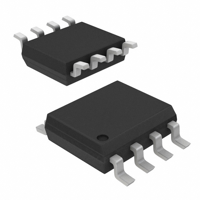
• Package: Plastic 8-pin SOIC Package (W)
The PI6C2502A features a low-skew, low-jitter, phase-locked loop
(PLL) clock driver. By connecting the feedback FB_OUT output
to the feedback FB_IN input, the propagation delay from the
CLK_IN input to any clock output will be nearly zero.
Logic Block Diagram
Product Pin Configuration
CLK_IN
Application
If a system designer needs more than 16 outputs with the features
just described, using two or more zero-delay buffers such as
PI6C2509Q, and PI6C2510Q, is likely to be impractical. The
device-to-device skew introduced can significantly reduce the
performance. Pericom recommends the use of a zero-delay buffer
and an eighteen output non-zero-delay buffer. As shown in Figure
1, this combination produces a zero-delay buffer with all the signal
characteristics of the original zero-delay buffer, but with as many
outputs as the non-zero-delay buffer part. For example, when
combined with an eighteen output non-zero delay buffer, a system
designer can create a seventeen-output zero-delay buffer.
AGND
CLK_OUT
PLL
FB_IN
FB_OUT
AVCC
1
FB_OUT
2
CLK_OUT
3
VCC
4
8-Pin
W
8
CLK_IN
7
AVCC
6
GND
5
FB_IN
Feedback
Buffer
PI6C2502
Reference
CLK_OUT
18 Output
Non-Zero
V
Zero Delay
Delay
17
Buffer
Clock
Signal
Figure 1. This Combination Provides Zero-Delay Between the
Reference Clocks Signal and 17 Outputs.
1
PS8500
10/02/00
�PI6C2502A
Phase-Locked
Loop
Clock
Driver
12345678901234567890123456789012123456789012345678901234567890121234567890123456789012345678901212345678901234567890123456789012123456789012
12345678901234567890123456789012123456789012345678901234567890121234567890123456789012345678901212345678901234567890123456789012123456789012
Pin Functions
Pin Name
Pin Numbe r
Type
D e s cription
CLK _IN
8
I
Reference Clock input. CLK _IN allows spread spectrum clock input.
FB_IN
5
I
Feedback input. FB_IN provides the feedback signal to the internal PLL.
FB_O UT
2
O
Feedback output FB_O UT is dedicated for external feedback.
FB_OUT has an embedded series- damping resistor of the same value
as the clock outputs CLK_OUT.
CLK _OUT
3
O
Clock outputs. These outputs provide low- skew copies of CLK_IN.
Each output has an embedded series- damping resistor.
AVC C
7
Power
Analog power supply. AVC C can be also used to bypass the PLL for
test purposes. When AVC C is strapped to ground, PLL is bypassed
and CLK_IN is buffered directly to the device outputs.
AGND
1
Ground
Analog ground. AGND provides the ground reference for the analog circuitry.
VC C
4
Power
Power supply.
GND
6
Ground
Ground.
DC Specifications (Absolute maximum ratings over operating free-air temperature range)
Symbol
Parame te r
M in.
VI
Input voltage range
VO
Output voltage range
M ax.
Units
VCC +0.5
0.5
V
VI_DC
DC input voltage
3.8
IO_DC
DC output current
100
mA
Power
Maximum power dissipation at TA = 55oC in still air
1.0
W
TSTG
Storage temperature
150
oC
65
Note:
Stress beyond those listed under absolute maximum ratings may cause permanent damage to the device.
Parame te r
Te s t Conditions
VCC
ICC
VI = VCC or GND; IO = 0(1) Standby Current
CI
VI = VCC or GND
CO
VO =VCC or GND
M in.
Typ.
3.6V
3.3V
M ax.
Units
10
µA
4
pF
6
Note:
1. Continuous Output Current
2
PS8500
10/02/00
�PI6C2502A
Phase-Locked
Loop
Clock
Driver
12345678901234567890123456789012123456789012345678901234567890121234567890123456789012345678901212345678901234567890123456789012123456789012
12345678901234567890123456789012123456789012345678901234567890121234567890123456789012345678901212345678901234567890123456789012123456789012
Recommended Operating Conditions
Symbol
Parame te r
M in.
M ax.
3.6
VCC
Supply voltage
3.0
VIH
High level input voltage
2.0
VIL
Low level input voltage
VI
Input voltage
0
VCC
TA
Operating free- air temperature
0
70
Units
V
0.8
ºC
Electrical Characteristics (Over Recommended Operating Free-Air Temperature Range
Pull Up/Down Currents of PI6C2502A, VCC = 3.0V)
Symbol
IOH
IOL
Parame te r
Condition
M in.
M ax.
Pull- up current
Vout = 2.4V
13.6
Pull- up current
Vout = 2.0V
22
Pull- down current
Vout = 0.8V
19
Pull- down current
Vout = 0.55V
13
Units
mA
AC Specifications
(Timing requirements over recommended ranges of supply voltage and operating free-air temperature)
Symbol
Parame te r
M in.
M ax.
Units
FCLK
Clock frequency PI6C2502A
80
134
MHz
DCYI
Input clock duty cycle
40
60
%
1
ms
Stabilization Time after power up
Switching Characteristics
(Over recommended ranges of supply voltage and operating free-air temperature, CL = 30pF)
Parame te r
From (Input)
tphase error without jitter
CLK_IN↑ at 100 & 66 MHz
Jitter, cycle- to- cycle
At 100 & 66 MHz
To (Output)
FB_IN↑
Duty cycle
CLK_OUT
tr, rise- time, 0.4V to 2.0V
tf, fall- time, 2.0V to 0.4V
VCC = 3.3V ±0.3V, 0-70°C
M in.
Typ.
M ax.
150
+150
75
+75
45
55
1.0
Units
ps
%
ns
1.1
Note:
These switching parameters are guaranteed by design.
3
PS8500
10/02/00
�PI6C2502A
Phase-Locked
Loop
Clock
Driver
12345678901234567890123456789012123456789012345678901234567890121234567890123456789012345678901212345678901234567890123456789012123456789012
12345678901234567890123456789012123456789012345678901234567890121234567890123456789012345678901212345678901234567890123456789012123456789012
Package Mechanical Information
Plastic 8-pin SOIC Package
8
3.78
3.99
.149
.157
4.80 .189
5.00 .196
1
.053
.068
.016
REF .026
0.406
0.660
SEATING PLANE
.0075
.0098
0.19
0.25
0.40 .016
1.27 .050
.2284
.2440
5.80
6.20
.013
.020
0.330
0.508
X.XX
X.XX
0.25
x 45˚
0.50
0-8˚
.0040 0.10
.0098 0.25
.050
BSC
1.27
.0099
.0196
1.35
1.75
DENOTES DIMENSIONS
IN MILLIMETERS
Ordering Information
Orde ring Code
Package Name
Package Type
Ope rating Range
PI6C2502AW
W8
8- pin 150- mil SOIC
Commercial
Pericom Semiconductor Corporation
2380 Bering Drive • San Jose, CA 95131 • 1-800-435-2336 • Fax (408) 435-1100 • http://www.pericom.com
4
PS8500
10/02/00
�
很抱歉,暂时无法提供与“PI6C2502AWE”相匹配的价格&库存,您可以联系我们找货
免费人工找货