PI6C49018
Low Power Networking Clock Generator
Features
Description
ÎÎ25 MHz crystal or clock input
The PI6C49018 is a clock generator device intended for PCIExpress/networking applications. The device includes four 100
MHz differential outputs for PCI-Express with low power HCSL
structure, one CMOS 125 MHz output, and one CMOS 66.66
MHz, and one CMOS 80 MHz output with spread spectrum.
ÎÎFour differential 100 MHz PCI-Express clock outputs – Low
O
power HCSL
ÎÎSpread spectrum capability on all 100 MHz PCI-e clock
outputs with -0.5% down spread
ÎÎOne single-ended 66.66 MHz output
ÎÎOne single-ended 125 MHz output for Gigabit Ethernet at
2.5V
ÎÎOne single-ended 80 MHz output with selectable down
spread
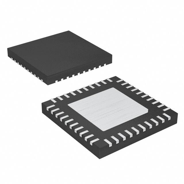
ÎÎ40-pin TQFN package
ÎÎOperating voltage 3.3 V ±5%
ÎÎIndustrial temperature (-40 to +85°C)
Block Diagram
O
BS
Using a serially programmable SMBus interface, the PI6C49018
incorporates spread spectrum modulation on the four 100 MHz
PCI-Express outputs with -0.5% down spread and the 80 MHz
output with selectable down spread.
E
T
LE
14-0209
1
www.pericom.com
PI6C49018
Rev. A
12/10/2014
�PI6C49018
Low Power Networking Clock Generator
VDD
PCIE0N
PCIE0
PCIE1
PCIE1N
VDD
VDD
GND
Cdd
PCIE2N
PCIE2
Pin Configuration
31
1
VDD
GND
VDD
PCIE3N
60M
PCIE3
GND
GND
VDD
VDD
GND
O
GND
VDD
BS
66.66M
SCLK
SDATA
125M
VDDO
X2
VDDX
X1
GNDX
GND
O
PD_RESET
VDD
VDD
11
80M
GND
VDD
21
40-pin QFN
Pin#
Pin Name
T
LE
Pin Description
Pin Type
Pin Description
VDD
Power
3.3V Supply Pin
2
GND
Power
Ground
3
VDD
Power
3.3V Supply Pin
4
PCIE3N
Output
Differential 100 MHz PCI Express Clock output
5
PCIE3
Output
Differential 100 MHz PCI Express Clock output
6
GND
Power
Ground
7
VDD
Power
3.3V Supply Pin
8
SCLK
Input
SMBus clock input
9
SDATA
I/O
SMBus data input
10
GND
Power
Ground
11
80M
Output
80 MHz LVCMOS output. Tri-state with weak pulldown when disabled
12
VDD
Power
3.3V Supply Pin
13
VDD
Power
3.3V Supply Pin
14
GNDX
Power
Ground
14-0209
2
www.pericom.com
E
1
PI6C49018
Rev. A
12/10/2014
�PI6C49018
Low Power Networking Clock Generator
Pin Description
Pin#
Pin Name
Pin Type
Pin Description
PD_RESET
Input
Global reset input powers down PLLs plus tri-states
outputs and sets the I2C tables to their default state
when pulled low. Controlled by external POR
16
X1
XI
Crystal input. Connect to 25 MHz fundamental mode
crystal or clock
17
X2
XO
Crystal output. Connect to 25 MHz fundamental mode
crystal. Float for clock input
18
VDDX
Power
3.3V Supply Pin for oscillator
19
VDDO
Power
125 MHz output supply voltage. Connect to +2.5 V
O
15
21
22
23
Output
125 MHz, +2.5 V LVCMOS output. Tri-stated with a
weak pull-down when disabled
GND
Power
Ground
VDD
Power
3.3V Supply Pin
66.66M
Output
66.66 MHz LVCMOS output. Tri-stated with a weak
pull-down when disabled
GND
Power
Ground
Power
3.3V Supply Pin
Power
Ground
Output
60 MHz LVCMOS output. Tri-state with weak pulldown when disabled
O
24
125M
BS
20
VDD
26
GND
27
60M
28
VDD
Power
3.3V Supply Pin
29
GND
Power
Ground
30
VDD
Power
3.3V Supply Pin
31
PCIE0N
Output
Differential 100 MHz PCI Express Clock output
32
PCIE0
Output
Differential 100 MHz PCI Express Clock output
33
PCIE1
Output
Differential 100 MHz PCI Express Clock output
34
PCIE1N
Output
Differential 100 MHz PCI Express Clock output
35
VDD
Power
3.3V Supply Pin
36
GND
Power
Ground
37
VDD
Power
3.3V Supply Pin
38
Cdd
Input
Input pin for off chip bypass capacitor. Connect to 0.01
μF capacitor
39
PCIE2N
Output
Differential 100 MHz PCI Express Clock output
40
PCIE2
Output
Differential 100 MHz PCI Express Clock output
3
www.pericom.com
E
14-0209
T
LE
25
PI6C49018
Rev. A
12/10/2014
�PI6C49018
Low Power Networking Clock Generator
Selection Table 1 – 80M Spread Spectrum
SS1
SS0
SSC
0
0
-1%
0
1
OFF
1
1
0
1
-0.5%
-0.75%
NOTE:
Refer to Byte0 control register.
Default setting is SS1:SS0 = 01
O
O
BS
E
T
LE
14-0209
4
www.pericom.com
PI6C49018
Rev. A
12/10/2014
�PI6C49018
Low Power Networking Clock Generator
Serial Data Interface (SMBus)
This part is a slave only SMBus device that supports indexed block read and indexed block write protocol using a single 7-bit address and read/write bit as shown below.
Address Assignment
A6
1
A5
A4
A3
A2
A1
A0
W/R
1
0
1
0
0
1
0/1
O
How to Write
1 bit
8 bits
D2H
Note:
1.
8 bits
1
8 bits
1
8 bits
1
Ack
Register
offset
Ack
Byte Count
=N
Ack
Data Byte
0
Ack
BS
Start
bit
1
…
8 bits
1
1 bit
Data Byte
N-1
Ack
Stop
bit
Register offset for indicating the starting register for indexed block write and indexed block read. Byte Count in write mode cannot be 0.
How to Read (M: abbreviation for Master or Controller; S: abbreviation for slave/clock)
1 bit
M:
Send
"D2h"
1 bit
S:
sends
Ack
8 bits
M: send
starting
databyte
location:
N
1 bit
1 bit
8 bits
S:
sends
Ack
M:
Start
bit
M:
Send
"D3h"
Bit
Description
7
Spread Select for 100 MHz push-pull
PCI-Express clocks
S:
sends
# of
data
bytes
that
will
be
sent:
X
S:
sends
Ack
1 bit
8 bits
1 bit
M:
sends
Ack
S:
sends
starting
data
byte
N
M:
sends
Ack
…
8 bits
1 bit
1 bit
…
S:
sends
data
byte
N+X-1
M:
Not
Acknowledge
M:
Stop
bit
Enables hardware or software control of OE bits
(see Byte 0-Bit 6 and Bit 5 Functionality table)
Software PD_RESET bit. Enables or disables all outputs.
(see Byte 0-Bit 6 and Bit 5 Functionality table)
Type
Power Up
Condition
Output(s)
Affected
RW
0
All 100MHz PCIExpress outputs
RW
0
PD_RESET, bit 5
RW
1
Notes
0=spread off
1 = -0.5% down
spread
0 = hardware cntl
1 = software ctrl
E
5
8 bits
T
LE
Byte 0: Spread Spectrum Control Register
6
1 bit
O
M:
Start
bit
8 bits
All outputs
0 = disabled
1 = enabled
80M
See Table 1 on Page4
4
Spread Select for 80MHz SS1
RW
0
3
Spread Select for 80MHz SS0
RW
1
2
OE for 66.66 MHz output
RW
1
66.66M
0 = disabled
1 = enabled
1
Reserved
R
-
-
-
0
OE for single-ended 125MHz
RW
1
Single-ended 125MHz
0 = disabled
1 = enabled
14-0209
5
www.pericom.com
PI6C49018
Rev. A
12/10/2014
�PI6C49018
Low Power Networking Clock Generator
Byte 0: Bit 6 and Bit 5 Functionality
Bit 6
Bit 5
Description
0
X
( PD_RESET= "H" will enable all outputs; SMBus cannot control each output.)
1
0
Disables all outputs and tri-states the outputs, PD_RESET HW pin/signal = DO NOT CARE
1
1
Enable outputs according to the SMBus default values; SMBus can control each output.
PD_RESET HW pin/signal = DO NOT CARE
O
Byte 1: Control Register
Description
Type
Power Up Condition
Output(s) Affected
7
OE for 80 MHz output
RW
1
80MHz
Reserved
R
-
-
0 = disabled
1 = enabled
-
Description
Type
Power Up Condition
Output(s) Affected
Notes
Reserved
R
-
-
-
6 to 0
BS
Bit
Notes
Byte 2: Control Register
Bit
O
7 to 0
Byte 3: Spread Spectrum Control Register
Power Up
Condition
Output(s)
Affected
RW
0
60M
R
-
RW
0
RW
1
100MHz HCSL
PCI-Express output
PCIE3
100MHz HCSL
PCI-Express output
PCIE2
R
-
OE for 100MHz HCSL
PCI-Express output PCIE1
RW
1
1
OE for 100MHz HCSL
PCI-Express output PCIE0
RW
1
0
Reserved
R
-
7
OE for 60MHz output
6
Reserved
5
OE for 100MHz HCSL
PCI-Express output PCIE3
4
OE for 100MHz HCSL
PCI-Express output PCIE2
3
Reserved
2
14-0209
Type
Notes
6
www.pericom.com
1 = enabled
0 = disabled
1 = enabled
0 = disabled
1 = enabled
0 = disabled
-
-
E
Description
T
LE
Bit
100MHz HCSL
PCI-Express output
PCIE1
100MHz HCSL
PCI-Express output
PCIE0
1 = enabled
0 = disabled
1 = enabled
0 = disabled
-
PI6C49018
Rev. A
-
12/10/2014
�PI6C49018
Low Power Networking Clock Generator
Byte 4: Control Register
Bit
Description
Type
Power Up Condition
Output(s) Affected
Notes
7 to 0
Reserved
R
-
-
-
Byte 5: Control Register
R
Power Up
Condition
0
Output(s)
Affected
-
Revision ID bit 2
R
0
-
-
5
Revision ID bit 1
R
0
-
-
4
Revision ID bit 0
R
0
-
-
Vendor ID bit 3
R
0
-
-
Vendor ID bit 2
R
0
-
-
Vendor ID bit 1
R
0
-
-
Vendor ID bit 0
R
0
-
-
Description
Type
7
Revision ID bit 3
6
O
Bit
2
1
0
Byte 6: Control Register
Bit
Description
7 to 0
Reserved
O
BS
3
Notes
-
Type
Power Up Condition
Output(s) Affected
Notes
R
-
-
-
E
T
LE
14-0209
7
www.pericom.com
PI6C49018
Rev. A
12/10/2014
�PI6C49018
Low Power Networking Clock Generator
Maximum Ratings
(Above which useful life may be impaired. For user guidelines, not tested.)
O
Maximum Supply Voltage, VDD............................................................... 7V
All Inputs and Outputs................................................. –0.5V to VDD +0.5V
Ambient Operating Temperature........................................ –40°C to +85°C
Storage Temperature......................................................... –65°C to +150°C
Junction Temperature.........................................................................125°C
Peak Soldering Temperature..............................................................260°C
ESD Protection (HBM).................................................................... 2000V
Note:
Stresses above the ratings listed below can cause permanent
damage to the PI6C49018. These ratings, which
are standard values for Pericom commercially rated parts,
are stress ratings only. Functional operation of the device at
these or any other conditions above those indicated in the
operational sections of the specifications is not implied.
Exposure to absolute maximum rating conditions for extended
periods can affect product reliability. Electrical
parameters are guaranteed only over the recommended
operating temperature range.
Recommended Operation Conditions
Parameters
Min.
-40
Power Supply Voltage (measured in respect to GND)
+3.135
Output Supply Voltage, VDDO
+2.25
Minimum Pulse Width of PD_RESET Input
100
BS
Ambient Operating Temperature
Typ.
3.3
Max.
Units
+85
°C
+3.465
V
+3.6
V
ns
DC Electrical Characteristics
Symbol
Operating Supply Voltage
VDD
Output Supply Voltage
VDDO
Input High Voltage
VIH
Input Low Voltage
VIL
Operating Supply Current
IDD at Output Disable
Condition
Short Circuit Current
Internal Pull-Up/PullDown Resistor
RPU/RPD
Output Capacitance
ZO
Input Capacitance
CIN
Min
Typ
Max
3.135
3.3
3.465
2.25
2.5
3.6
X1/SCLK, SDATA
2
VDD
X1/SCLK, SDATA
–0.3
0.8
IDD
No load, all supply pins, PD_RESET = 1
50
IDDPD
PD_RESET = 0
1
All single-ended clocks
±35
PD_RESET
240
All single-ended clocks
110
IOS
All input pins
8
www.pericom.com
75
PI6C49018
Units
V
105
mA
kΩ
30
pF
6
Ω
Rev. A
12/10/2014
E
14-0209
Conditions
T
LE
Parameter
O
Unless otherwise specified, VDD=3.3V±10%, VDDO=2.5V,Ambient Temperature –40°C to +85°C
�PI6C49018
Low Power Networking Clock Generator
Electrical Characteristics - Single-Ended
Unless otherwise specified, VDD=3.3V±10%, VDDO=2.5V, Ambient Temperature –40°C to +85°C
Parameter
Symbol
Input Clock Frequency
Conditions
Min
Typ
FIN
Output Frequency Error
tOR
Output Fall Time
tOF
O
Output Rise Time
Output Clock Duty Cycle
At VDD/2
Max
Units
25
MHz
0
ppm
0.5
0.7 V to 1.7V 125 MHz
1
0.4
At VDD/2
0.5
1
Measured at VDD/2, 125MHz
47
50
53
Measured at VDD/2, all other
outputs
45
50
55
ns
%
BS
Output High Voltage
VOH
IOH = -4mA
VDD-0.4
V
Output High Voltage
VOH
IOH = -8mA
2.4
V
Output Low Voltage
VOL
IOL = 4mA
0.4
V
Output Low Voltage
VOL
IOL = 8mA
0.4
V
60MHz clock output
200
ps
125MHz clock output
60M/66.66M/80MHz clock
output
60M/66.66 MHz, 500 kHz
offset
80MHz clock output
±100
Cycle-to-Cycle Jitter
Modulation Rate
Clock Stabilization Time
from Power Up
Note 1: CL = 15 pF
Note 2: Cycle-to-cycle jitter is measured at 25°C.
Note 3: Spread OFF.
125MHz clock output
±100
±250
T
LE
Phase Noise
±150
O
Peak-to-Peak Jitter
66.66MHz clock output
PD_RESET goes high to 1% of
final frequency
-100
32
3
dB
60
kHz
10
ms
E
14-0209
9
www.pericom.com
PI6C49018
Rev. A
12/10/2014
�PI6C49018
Low Power Networking Clock Generator
Electrical Characteristics - 100MHz Differential HCSL Outputs
Unless otherwise specified, VDD=3.3V±10%, Ambient Temperature –40°C to +85°C
Parameter
Symbol
Conditions
Min
Typ
Output Frequency
Cycle-to-Cycle Jitter
TCC/Jitter
Peak-to-Peak Phase Jitter
Units
100
MHz
150
TJø
PCIe Gen1 filter function
86
Spread Range
O
Spread Rate
Duty Cycle
Max
45
TDC
Clock Stabilization from Power Up
ps
-0.5
0
%
32
0
kHz
50
55
%
3.5
ms
Note3, 4
0.6
4.0
V/ns
Falling Edge Rate
Note3, 4
0.6
4.0
V/ns
Rise-Fall Matching
Note3, 11
VT = 50%(measurement threshold), Intra-pair skew
50
ps
VT = 50%(measurement threshold), Inter-pair skew
200
ps
Output Skew
BS
Rising Edge Rate
Impedance(Zo)
High-Level Output
Low-Level Output Voltage
Absolute Crossing Point Voltage
Variation of VCROSS over all rising clock edges
Average Clock Period Accuracy
17
ZC-DC
VOH
Note2 (Rs = 33ohm)
0.65
0.71
T
LE
Voltage
O
Clock Source DC
TOSKEW
20%
Absolute Period (including jitter and spread spectrum)
-0.20
VOL
VCROSS
Note2, 5, 6
VCROSS
0
0.25
Note2, 5, 8
Delta
TPERIOD
AVG
TPERIOD
0.85
V
0.05
V
0.55
V
140
mV
Note3, 9, 10
-300
2800
ppm
Note3, 7
9.847
10.203
ns
E
ABS
Ω
NOTE:1.Measured at the end of an 8-inch trace with a 5pF load.
2.Measurement taken from a single-ended waveform.
3.Measurement taken from a differential waveform.
4.Measured from -150 mV to +150 mV on the differential waveform. The signal is monotonic through the measurement region for rise and fall time. The 300 mV
measurement window is centered on the differential zero crossing.
5.Measured at crossing point where the instantaneous voltage value of the rising edge of 100M+ equals the falling edge 100M-.
6.Refers to the total variation from the lowest crossing point to the highest, regardless of which edge is crossing. Refers to all crossing points for this measurement.
7.Defines as the absolute minimum or maximum period. This includes cycle-to-cycle jitter, relative PPM tolerance, and spread spectrum modulation.
8.Defined as the total variation of all crossing voltages of rising 100M+ and falling 100M-.
9.Refer to section 4.3.2.1 of the PCI Express Base Specification, Revision 1.1 for information regarding PPM considerations.
10.PPM refers to parts per million and is a DC absolute period accuracy specification. 1 PPM is 1/1,000,000th of 100 MHz exactly or100 Hz. For 300 PPM there is an
error budget of 100Hz/PPM * 300 PPM = 30 kHz. The period is measured with a frequency counter with measurement window set at 100 ms or greater. With spread
spectrum turned off the error is less than ±300 ppm. With spread spectrum turned on there is an additional +2500 PPM nominal shift in maximum period resulting
from the -0.5% down spread.
11.Matching applies to rising edge rate for PCIe and falling edge rate for PCIeN. It is measured using a ±75 mV window centered on the median cross point where
14-0209
10
www.pericom.com
PI6C49018
Rev. A
12/10/2014
�PI6C49018
Low Power Networking Clock Generator
Application Notes
Crystal circuit connection
The following diagram shows PI6C49018 crystal circuit connection with a parallel crystal. For the CL=18pF crystal, it is suggested
to use C1= 27pF, C2= 27pF. C1 and C2 can be adjusted to fine tune to the target ppm of crystal oscillator according to different
board layouts.
Crystal Oscillator Circuit
O
XTAL_IN
C1
27pF
SaRonix-eCera
FL2500047
Crystal�(CL�=�18pF)
BS
XTAL_OUT
C2
27pF
O
E
T
LE
Recommended Crystal Specification
Pericom recommends:
a) FY2500081, SMD 5x3.2(4P), 25M, CL=18pF, +/-30ppm, http://www.pericom.com/pdf/datasheets/se/FY_F9.pdf
b) FL2500047, SMD 3.2x2.5(4P), 25M, CL=18pF, +/-20ppm, http://www.pericom.com/pdf/datasheets/se/FL.pdf
14-0209
11
www.pericom.com
PI6C49018
Rev. A
12/10/2014
�PI6C49018
Low Power Networking Clock Generator
Configuration test load board termination for HCSL Outputs
Rs
33Ω
5%
PI6C49018
Clock
TLA
O
Rs
33Ω
5%
Clock#
TLB
2pF
5%
2pF
5%
BS
Figure 4. Configuration Test Load Board Termination
O
E
T
LE
14-0209
12
www.pericom.com
PI6C49018
Rev. A
12/10/2014
�PI6C49018
Low Power Networking Clock Generator
Packaging Mechanical: 40- TQFN (ZD)
O
O
BS
T
LE
Note:
• For latest package info, please check: http://www.pericom.com/products/packaging/mechanicals.php
Ordering Code
Package Code
PI6C49018ZDIE
ZD
E
Ordering Information(1-3)
Package Description
40-contact, Thin Fine Pitch Quad Flat No-Lead (TQFN)
Notes:
1. Thermal characteristics can be found on the company web site at www.pericom.com/packaging/
2. E = Pb-free and Green
3. Adding an X suffix = Tape/Reel
Pericom Semiconductor Corporation • 1-800-435-2336 • www.pericom.com
14-0209
All trademarks are property of their respective owners.
13
www.pericom.com
PI6C49018
Rev. A
12/10/2014
�


 工商网监
湘ICP备2023018690号
工商网监
湘ICP备2023018690号
