PI6LC4820
HiFlexTM Ethernet Network Clock Generator
Features
Description
ÎÎ3.3V supply voltage
The PI6LC4820 is an LC VCO based low phase noise design
intended for 10GbE applications. Typical 10GbE usage assumes
a 25Mhz crystal input, while the PLL loop is used to generate
the 156.25MHz outputs. An additional buffered crystal oscillator output is provided to serve as a low noise reference for other
circuitry.
ÎÎCrystal input: 25 MHz
ÎÎDifferential input: 25MHz, 156.25 MHz
ÎÎOutput frequencies of 312.5, 156.25, 125MHz supported
ÎÎ9 LVPECL or LVDS bank selectable outputs
ÎÎLow 1ps max integrated phase noise design
For Ethernet applications other than 10GbE, programmable
dividers allow for simultaneous output of 312.5, 156.25, and
125MHz.
(12kHz to 20MHz)
ÎÎOptional xtal or clock input selection
ÎÎPLL Bypass mode for test
ÎÎPower supply noise rejection: -50 dBc typical @ 156.25 MHz
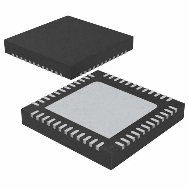
ÎÎPackaging (Pb-free & Green): 48-lead 7×7mm TQFN
FS0
QB_Mode
QA_Mode0
QB2+
QB2-
QB1+
QB1-
QB0+
QB0-
46
45
44
43
42
41
40
39
38
VDD_QB
IN-
47
37
36
VDD_QA
X1
2
35
QA0+
X2
3
34
QA0-
VDD_OSC
4
33
QA1+
IN_SEL
5
32
QA1-
PLL_BYPS
6
31
QA2+
GND
7
30
QA2-
FS1
8
29
QA3+
QC_Mode
9
28
QA3-
VDDA
10
27
QA4+
GND
11
26
QA4-
25
VDD_QA
GND
14
15
16
17
18
19
20
21
22
23
24
FS_B
GND
FS_A
GND
FS_C
QA_Mode1
VDD
GND
QC-
QC+
VDD_QC
12
13
GND
VDD_PLL
13-0167
48
1
IN+
IN_SE
Pin Configuration
1
PI6LC4820 Rev D
11/13/13
�PI6LC4820
HiFlexTM Ethernet Network Clock Generator
Block Diagram
VDD_OSC
IN_SEL
FS0
VDD
FS_A
VDD_PLL
PLL_BYPS
VDD_QA QA_Mode0
X1
Crystal
Oscillator
SaRonix-eCera
GC25000-76B
1
X2
IN_SE
QA0+
QA0QA1+
QA1QA2+
QA2-
0
CMOS
NC
÷M
PFD
CHARGE/
LC_VCO
F_VCO
÷A
0/NC
QA3+
QA3QA4+
QA4-
IN+
IN-
DIFF.
1
÷N
QA_Mode1
VDD_QB
QB_Mode
QB0+
QB0QB1+
QB1QB2+
QB2-
1
POR
÷B
0/NC
VDD_QC
QC+
QC-
1
÷C
FS1
13-0167
2
FS_B
FS_C
NC
0
VDD_QC
QC_Mode
PI6LC4820 Rev D
11/13/13
�PI6LC4820
HiFlexTM Ethernet Network Clock Generator
Pin Description
Pin Number Pin Name
Type
Description
1
FS0
Input (LVCMOS)
Frequency Select Pin. Use FS0=FS1=0 for all 25MHz input sources.
Internal pull-down is 100K-Ohm
2
X1
Input
Crystal input pin. No internal xtal load capacitance
3
X2
Output
Crystal output pin. No internal xtal load capacitance
4
VDD_OSC
Power
VDD for reference oscillator
5
IN_SEL
Input (LVCMOS)
Input mux selection pin
6
PLL_BYPS
Input (LVCMOS)
Optional mode to bypass PLL and have input reference source connect
directly to outputs
7
GND
Power
Ground pin
8
FS1
Input (LVCMOS)
Frequency Select Pin. Use FS0=FS1=0 for all 25MHz input sources.
Internal pull-down is 100K-Ohm
9
QC_Mode
Input (LVCMOS)
Out mode control pin selects LVPECL or LVDS mode. If left floating,
outputs are tri-stated
10
VDDA
Power
VDD for analog circuitry
11
GND
Power
Ground pin
12
VDD_PLL
Power
VDD for PLL.
13
GND
Power
Ground pin
14
FS_B
Input (LVCMOS)
Frequency Select Pin for Bank B, Output Divider
15
GND
Power
Ground pin
16
FS_A
Input (LVCMOS)
Frequency Select Pin for Bank A, Output Divider
17
GND
Power
Ground pin
18
FS_C
Input (LVCMOS)
Frequency Select Pin for Bank C, Output Divider
19
QA_Mode1
Input (LVCMOS)
Out mode control pin selects LVPECL or LVDS mode. If left floating,
outputs are tri-stated
20
VDD
Power
VDD
21
GND
Power
Ground pin
22,
QC-,
23
QC+
Output (Differential)
Bank C LVDS/LVPECL selectable output. Controlled by QC_Mode pin
24
VDD_QC
Power
VDD for bank C outputs
25
VDD_QA
Power
VDD for bank A outputs
26,
QA4-,
27
QA4+
Output (Differential)
Bank A LVDS/LVPECL selectable output. Controlled by QA_Mode1 pin
28,
QA3-,
29
QA3+
Output (Differential)
Bank A LVDS/LVPECL selectable output. Controlled by QA_Mode1 pin
30,
QA2-,
31
QA2+
Output (Differential)
Bank A LVDS/LVPECL selectable output. Controlled by QA_Mode0 pin
13-0167
3
PI6LC4820 Rev D
11/13/13
�PI6LC4820
HiFlexTM Ethernet Network Clock Generator
Pin Description (Continued..)
Pin Number Pin Name
Type
Description
Output (Differential)
Bank A LVDS/LVPECL selectable output. Controlled by QA_Mode0 pin
Output (Differential)
Bank A LVDS/LVPECL selectable output. Controlled by QA_Mode0 pin
32,
QA1-,
33
QA1+
34,
QA0-,
35
QA0+
36
VDD_QA
Power
VDD for bank A outputs
37
VDD_QB
Power
VDD for bank B outputs
38,
QB0-,
39
QB0+
Output (Differential)
Bank B LVDS/LVPECL selectable output. Controlled by QB_Mode pin
40,
QB1-,
41
QB1+
Output (Differential)
Bank B LVDS/LVPECL selectable output. Controlled by QB_Mode pin
42,
QB2-,
43
QB2+
Output (Differential)
Bank B LVDS/LVPECL selectable output. Controlled by QB_Mode pin
44,
QA_Mode0,
45
QB_Mode
Input (LVCMOS)
Out mode control pins select LVPECL, LVDS mode. If left floating,
outputs are tri-stated
46
IN-
Input (Differential)
Frequency input pin, differential (accepts: LVDS, LVPECL, HCSL)
47
IN+
Input (Differential)
Frequency input pin, differential (accepts: LVDS, LVPECL, HCSL)
48
IN_SE
Input
Frequency input pin, Single Ended
Input Mux Selection
IN_SEL
Input
0
Select Crystal Input (Pins 2, 3)
1
Select IN+, IN- Differential Input (Pins 46, 47)
NC
Select IN_SE LVCMOS Input (pin 48)
PLL Bypass Control Function
PLL_BYPS
PLL operation
0
PLL enabled
1
PLL bypassed
NC
PLL enabled for Banks A, B; Bank C is driven directly by the output of the input mux.
Input Divider Control Table
FS0
Divider Ratio
0
1
1
5
13-0167
4
PI6LC4820 Rev D
11/13/13
�PI6LC4820
HiFlexTM Ethernet Network Clock Generator
PLL Feedback Divider Control Table
FS1
Feedback Divider Ratio
0
25
1
20
Output Frequency Control Table
FS_A
FS_B
FS_C
Output Frequency
0
0
0
156.25
1
1
1
125
NC
NC
NC
312.5
Bank A Output Control
QA_Mode0
QA[2:0]
QA_Mode1
QA[4:3]
0
LVDS
0
LVDS
1
LVPECL
1
LVPECL
NC
Hi-Z
NC
Hi-Z
Bank B Output Control
QB_Mode
QB[2:0]
0
LVDS
1
LVPECL
NC
Hi-Z
C-bank Output Interface Control Configuration
QC_Mode
QC+/-
0
LVDS
1
LVPECL
NC
Hi-Z
13-0167
5
PI6LC4820 Rev D
11/13/13
�PI6LC4820
HiFlexTM Ethernet Network Clock Generator
Maximum Ratings
(Above which useful life may be impaired. For user guidelines, not tested.)
Storage Temperature........................................................... –65°C to +150°C
Supply Voltage to Ground Potential, VDD .......................–0.5V to +4.6V
ESD Protection (HBM) ...................................................................... 2000 V
Note: Stresses greater than those listed under MAXIMUM
RATINGS may cause permanent damage to the device. This is a
stress rating only and functional operation of the device at these
or any other conditions above those indicated in the operational
sections of this specification is not implied. Exposure to absolute
maximum rating conditions for extended periods may affect
reliability.
Operating Conditions
Symbol
Parameters
Min.
Max.
Units
VDD
General Power Supply Voltage
3.0
3.6
V
TA
Ambient Temperature
–40
85
°C
IDD
Power Supply Current
All outputs loaded
425
IDD_ A
Power Supply Current for pin10
13
IDD_PLL
Power Supply Current for pin12
30
VDDA
Analog Power Supply Voltage
2.7
3.6
VDD_PLL
PLL Power Supply Voltage
2.7
3.6
mA
V
LVCMOS Input Electrical Characteristics
Symbol
Parameters
Conditions
Min.
Typ.
Max.
VIH
Input High Voltage
VIL
Input Low Voltage
VIH
Input High Current
IN_SEL, PLL_BYPS,
VIL
Input Low Current
FS_A, FS_B, FS_C,
QA_Mode, QB_Mode,
QC_Mode
0.8
V
IIH
Input High Current
VIN = VDD
45
mA
IIL
Input Low Current
VIN = 0V
Rpu
Internal pull up resistance
100
KW
Rdn
Internal pull down resistance
100
KW
TDC
Input Duty Cycle
CIN
Input Capacitance1
FIN
Input Frequency
2
FS0, FS1
V
0.8
V
2.6
V
µA
-45
35
65
%
1.5
15
Units
pF
160
MHz
Note:
1. There is no internal load capacitance built in to the X1 and X2 pins
13-0167
6
PI6LC4820 Rev D
11/13/13
�PI6LC4820
HiFlexTM Ethernet Network Clock Generator
Differential Input Characteristics
Symbol
Parameters
Conditions
Min.
VIH
Input High Voltage
VIL
Input Low Voltage
VDD - 2.0
VCM
Input Bias Voltage
VDD - 1.8
VDD / 2
100
R IN
Input Differential Impedence2
80
VIN-PP
Input Differential Swing
0.3
CIN
Differential Input Capacitance
Typ.
Max.
Units
VDD - 0.7
V
V
V
120
W
1.8
VPP
1.5
pF
Note:
1. 2. Differential input can be AC or DC coupled.
LVPECL Output Characteristics (Over Operating Conditions. See Fig. 1 and 2 for load conditions.)
Symbol
Parameters
Condition
FOUT
Output Frequency
Trise / Tfall
Rise and Fall Time
20% to 80%, singleended
TDC
Duty Cycle
Differential
Jphase
Integrated phase jitter
12KHz-20MHz
@ 156.25MHz,
25MHz Xtal input
TDIS
Min.
Typ.
Max.
Units
312.5
MHz
400
ps
53
%
1
ps rms
Output Disable Time
80
ns
TEN
Output Enable Time
80
ns
TLOCK
PLL Lock Time
2
ms
VPP
Output peak-peak Voltage
Single-ended
0.6
1
V
VOH
Output High Voltage
VDD = 3.3V
VDD-1.4
VDD-0.9
V
VOL
Output Low Voltage
VDD = 3.3V
VDD-2.0
VDD-1.7
V
25
47
0.54
LVDS Output Characteristics (Over Operating Conditions See Fig. 1 and 2 for load conditions.)
Symbol
Parameters
FOUT
Output Frequency
Trise / Tfall
Rise and Fall Time
20% to 80%, singleended
TDC
Duty Cycle
Differential
Jphase
Integrated phase jitter
12KHz-20MHz
@ 156.25MHz,
25MHz Xtal input
13-0167
Condition
Min.
Typ.
25
7
47
0.54
Max.
Units
312.5
MHz
270
ps
53
%
1
ps rms
PI6LC4820 Rev D
11/13/13
�PI6LC4820
HiFlexTM Ethernet Network Clock Generator
LVDS Output Characteristics (Continued..)
Symbol
Parameters
TDIS
Output Disable Time
80
TEN
Output Enable Time
80
TLOCK
PLL Lock Time
2
|VAMP|1
Differential Output Voltage Amplitude
Condition
Min.
|VOH - VOL| with
100Ω external termination
250
|VOH - VOL| with
120Ω external termination
250
Typ.
Max.
Units
ns
ms
520
mV
600
VOH
Output High Voltage
1.8
VOL
Output Low Voltage
0.925
VOS
Output offset voltage
1.125
1.375
ROL
Differential output impedance
85
140
V
Ω
Note:
1. Valid for part numbers with date code after Y1338.
Power Supply Noise Rejection Specification
Parameter
Conditions
Supply Noise induced
phase spur @ 156.25
NHz output (see note)
Fm = 100kHz to 400KHz
Min.
typ
Max.
Units
-50
dBc
Note:
1. Measured with 50mVp-p Sinusoidal Interference on the supply VDDQx, measured with the supply filter as shown in Figure 2.
Crystal Characteristic (link to "http://www.pericom.com/saronix" for more detailed crystal specifications)
Parameters
Description
Min
OSCmode
Mode of Oscillation
Fundamental
FREQ
Frequency
(1)
Typ
Max.
25
Units
MHz
ESR
Equivalent Series Resistance
50
Cload
Load Capacitance
Cshunt
Shunt Capacitance
7
pF
Drive Level
0.1
mW
18
Ohm
pF
Note:
1. ESR value is dependent upon frequency of oscillation
13-0167
8
PI6LC4820 Rev D
11/13/13
�PI6LC4820
HiFlexTM Ethernet Network Clock Generator
Figure 1. Test Circuit
3.3V ± 5%
VDDQx
VDDA
0.1µF
10.5Ω
VDD_PLL
0.1µF
10µF
Figure 2. Power Supply Filter
Application Notes
PI6LC4820 is a high performance and low jitter clock generator for advanced Gigabit Ethernet systems. It has three independent
banks whose outputs can be set to LVPECL or LVDS and in 3 outputs frequencies : 125MHz, 156.25MHz, and 312.5MHz. It is critical to ensure the power supply is properly decoupled and the layout around the crystal is properly routed to achieve this low jitter
performance. The following guide is highly recommended to be adopted into the system PCB designs.
m
13-0167
9
PI6LC4820 Rev D
11/13/13
�PI6LC4820
HiFlexTM Ethernet Network Clock Generator
Power Decoupling Schematic
U1
Place to pin
VDD
R1
2. 2_603
2.2uF C3
VDD
C5
0.1uF
R2
2. 2_603
VDD
C4
1uF
2.2uF C6
C7
0.1uF
QA_MODE_1
19
FS_A
QA_MODE_0
16
44
VDD_QA
36
25
QB_MODE
FS_B
45
14
VDD_QB
37
QC_MODE
FS_C
9
18
VDD_QC
R3
2. 2_603
2.2uF C8
C9
0.1uF
24
INPUT_P
INPUT_N
47
46
IN_SE
IN_SELECT
48
5
FS_1
FS_0
8
1
PLL_BY PASS
6
2
3
Y1
25M (CL=18p)
C1
27p
C2
33p
4
QA_MODE1
QA4+
QA4-
FS_A
QA_MODE0
QA3+
QA3-
VDD_QA2
VDD_QA1
QA2+
QA2-
QA_MODE
FS_B
QA1+
QA1QA0+
QA0-
VDD_QB
QB2+
QB2-
QC_MODE
FS_C
QB1+
QB1-
VDD_QC
QB0+
QB0-
IN+
IN-
QC0+
QC0-
IN_SE
IN_SEL
VDDA
VDD_PLL
FS_1
FS_0
VDD
PLL_BY PS
GND6
GND5
GND4
GND3
GND2
GND1
EP
X1
X2
VDD_OSC
27
26
CLK_QA4_P
CLK_QA4_N
29
28
CLK_QA3_P
CLK_QA3_N
31
30
CLK_QA2_P
CLK_QA2_N
33
32
CLK_QA1_P
CLK_QA1_N
35
34
CLK_QA0_P
CLK_QA0_N
43
42
CLK_QB2_P
CLK_QB2_N
41
40
CLK_QB1_P
CLK_QB1_N
39
38
CLK_QB0_P
CLK_QB0_N
22
23
CLK_QC0_P
CLK_QC0_N
C10
0.01uF
OA4_P
QA4_N
C11
R4
150
R5
150
To LVPECL
eq. 100 termination
0.01uF
Place to pin
VDD
R6
10_802
C15
C12
0.1uF
22uF
VDD
10
R2
12
20
4. 7_603
VDD
C14
0.1uF
21
17
15
13
11
7
49
PI6LC4820
R7
4. 7_603
C15
22uF
VDD
Place to pin
R8
2. 2_603
C16
0.1uF
C15
22uF
1) It is suggested to use the schematic’s decoupling RC value to get best board noise filtering
2) Typical LVPECL is using 150W pull down in AC or DC coupling drive according to ASIC ref_clk I/O spec
3) The crystal circuit C1/C2 load values are for CL=18pF crystal, they can be adjusted for other CL crystals
4) Please refer to the datasheet for other static I/O logic set for the request work modes and output frequencies
13-0167
10
PI6LC4820 Rev D
11/13/13
�PI6LC4820
HiFlexTM Ethernet Network Clock Generator
Crystal circuit connection
The following diagram shows PI6LC4820 crystal circuit connection with a parallel crystal. For the CL=18pF crystal, it is suggested
to use C1=27pF, C2=33pF. C1 and C2 can be adjusted to fine tune to the target ppm of crystal oscillator according to different board
layouts.
Crystal Oscillator Circuit
X1
C1
27pF
SaRonix-eCera
GC2500076B
Crystal�(CL�=�18pF)
X2
C2
33pF
2. PI6LC4820 Crystal Circuit Layout Guide
Crystal Circuit Oscillator
GND Pad
Pin name
1 FS0
2 X1
8 8
7 7
6 6
5 5
4 4
5 IN_SEL
2 2
1 1
4 VDD_OSC
3 3
3 X2
6 PLL-BYBS
7 GND
8 FS1
GND via
C1 cap. pad
Crystal pad
4
Copyright Pericom Semiconductor 2007
PCB Layers:
L_1 Signal (Top)
Board via
L_2 GND plane
keep out area
Solder pad
PERICOM CONFIDENTIAL INFORMATION
Last Slide
Recommended Crystal Specification
Pericom recommends:
a) GC2500003 XTAL 49S/SMD(4.0 mm), 25M, CL=18pF, +/-30ppm, http://www.pericom.com/pdf/datasheets/se/GC_GF.pdf
b) FY2500081, SMD 5x3.2(4P), 25M, CL=18pF, +/-30ppm, http://www.pericom.com/pdf/datasheets/se/FY_F9.pdf
c) FL2500047, SMD 3.2x2.5(4P), 25M, CL=18pF, +/-20ppm, http://www.pericom.com/pdf/datasheets/se/FL.pdf
13-0167
11
PI6LC4820 Rev D
11/13/13
�PI6LC4820
HiFlexTM Ethernet Network Clock Generator
Crystal Layout Example
2. PI6LC4820 Crystal Circuit Layout Guide
GND Pad
Pin name
1 FS0
2 X1
8 8
7 7
6 6
5 5
4 4
5 IN_SEL
2 2
1 1
4 VDD_OSC
3 3
3 X2
6 PLL-BYBS
7 GND
8 FS1
GND via
C1 cap. pad
Board via
Crystal pad
keep out area
GND via
trace L_1
1) X1 pin is the most sensitive as crystal amplifier input
6
PCB Layers:
L_1 Signal (Top)
Copyright Pericom Semiconductor 2007
L_2 GND plane
Solder pad
PERICOM CONFIDENTIAL INFORMATION
Last Slide
2) X1 and X2 pins connected to crystal trace loop should be very narrow without any board via in
the loop and keep the via out of the area
3) Place crystal as close to the IC as possible along with C1/C2 load caps. There should be no via at the top layer to the crystal
4) Keep crystal load cap. C1/C2 to GND sides as close as possible so that the minimum board noise could be coupled into the caps
4. VDD and GND Pins Layout
1) Small value decoupling caps. (0.1uF, 1uF, and 2.2uF) should be placed close to each VDD pin or via
2) Each GND pin should have its own via to the common GND plane
3) Thermal pad must be connected to the GND plane for better thermal distribution and signal conducting with reasonable via
counts (>6)
5. LVPECL Differential Output Layout
1) 150W pull-down should be put close to clock output side with symmetrical position in one pair
2) Do not share 150W pull-down GND via between each pairs
6. Differential Input
1) This device differential input (pin 47, 48) can accept 25MHz, 125MHz, and 156.25MHz frequencies in most common differential
signals (LVPECL, LVDS, HCSL etc.) in either AC or DC coupling, with proper IN_SEL, FS0, and FS1 setting
2) The device differential input has equivalent 100W differential termination on chip, so PCB 100W external termination is normally
not necessary.
13-0167
12
PI6LC4820 Rev D
11/13/13
�PI6LC4820
HiFlexTM Ethernet Network Clock Generator
Packaging Mechanical: 48-Pin TQFN (ZD)
1
DATE: 05
3/09/12
4
Notes:
1. All dimensions are in millimeters, angles are in degrees.
2. Refer JEDEC MO-220/VKKD
3. Thermal Pad Soldering Area
4. Depending on the method of lead termination at the edge of the package,
pull back maybe present.
DESCRIPTION: 48-Contact, Thin Fine Pitch Quad Flat No-Lead (TQFN)
PACKAGE CODE: ZD (ZD48)
REVISION: E
DOCUMENT CONTROL #: PD-2045
12-0458
Note:
1. • For latest package info, please check: http://www.pericom.com/products/packaging/mechanicals.php
Ordering Information(1-3)
Ordering Code
Package Code
Package Description
PI6LC4820ZDE
ZD
48-Pin, Pb-free & Green (TQFN)
Notes:
1. Thermal characteristics can be found on the company web site at www.pericom.com/packaging/
2. E = Pb-free and Green
3. 3. Adding an X suffix = Tape/Reel
Pericom Semiconductor Corporation • 1-800-435-2336 • www.pericom.com
13-0167
13
PI6LC4820 Rev D
11/13/13
�