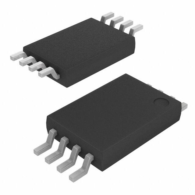
PI6LC48C21
Single Output LVCMOS Clock Generator
Features
Description
ÎÎSingle
The PI6LC48C21 is a single LVCMOS output synthesizer optimized to generate Ethernet reference clock frequencies and is a
member of Pericom’s HiFlex family of high performance clock
solutions. Using a 25MHz crystal, It can generate 125MHz with
very low phase jitter.
LVCMOS output
ÎÎSupports 125MHz or 130MHz output frequencies
ÎÎRMS phase jitter @ 125MHz, using a 25MHz crystal
(1.875MHz – 20MHz): 0.15ps (typical)
ÎÎRMS phase jitter @ 125MHz, using a 25MHz crystal
It is ideal for Ethernet interface in all kind of systems.
(12kHz – 20MHz): 0.33ps (typical)
ÎÎFull 3.3V or 2.5V supply modes
ÎÎIndustrial ambient operating temperature
ÎÎAvailable in lead-free package: 8-TSSOP
Applications
ÎÎNetworking systems
Block Diagram
Pin Configuration
OE
XTAL_IN
OSC
XTAL_OUT
PFD
VCO
/5
CLK
/25
15-0105
1
VDDA
1
8
VDD
OE
2
7
CLK
XTAL_OUT
3
6
GND
XTAL_IN
4
5
NC
www.pericom.com
PI6LC48C21
Rev. B
08/04/15
�PI6LC48C21
Single Output LVCMOS Clock Generator
Pinout Table
Pin No.
Pin Name
I/O Type
Description
1
VDDA
Power
Analog Power Supply
2
OE
Input
3, 4
XTAL_OUT,
XTAL_IN
Crystal
5
NC
6
GND
Power
Ground
7
CLK
Output
Output Clock
8
VDD
Power
Power Supply
Pull-up
High: Output enabled; Low: Output high impedence
Crystal Input and Output
No Connect
Typical Crystal Requirement
Parameter
Minimum
Maximum
Units
27.2
MHz
Equivalent Series Resistance
(ESR)
50
Ω
Shunt Capacitance
7
pF
Drive Level
1
mW
Mode of Oscillation
Frequency
Typical
Fundamental
22.4
25
Recomended Crystal Specification
Pericom recommends:
a) FL2500047, SMD 3.2x2.5(4P), 25MHz, CL=18pF, +/-20ppm. http://www.pericom.com/pdf/datasheets/se/FL.pdf
b) FY2500091, SMD 5x3.2(4P), 25MHz, CL=18pF, +/-30ppm. http://www.pericom.com/pdf/datasheets/se/FY_F9.pdf
c) FL2600018, SMD 3.2x2.5(4P), 26MHz, CL=18pF, +/-20ppm. http://www.pericom.com/pdf/datasheets/se/FL.pdf
Output Frequency
Crystal Frequency (MHz)
Output Frequency (MHz)
25
125
26
130
Pin Characteristics
Symbol
Parameter
Minimum
Typical
Maximum
Units
CJN
Input Capacitance
4
pF
R PULLUP
Pull up resistor
51
kΩ
ROUT
Output Impedence
15
Ω
15-0105
2
www.pericom.com
PI6LC48C21
Rev. B
08/04/15
�PI6LC48C21
Single Output LVCMOS Clock Generator
Maximum Ratings (Over operating free-air temperature range)
Note:
Stresses greater than those listed under MAXIMUM
RATINGS may cause permanent damage to the device. This
is a stress rating only and functional operation of the device
at these or any other conditions above those indicated in
the operational sections of this specification is not implied.
Exposure to absolute maximum rating conditions for
extended periods may affect reliability.
Storage Temperature............................................... -65ºC to+155ºC
Ambient Temperature with Power Applied..........-40ºC to+85ºC
3.3V Analog Supply Voltage.......................................-0.5 to +3.6V
ESD Protection (HBM).......................................................... 2000V
DC Electrical Characteristics
Power Supply DC Characterisitcs, (VDD = VDDA , TA = -40 to 85ºC)
Symbol
Parameter
VDD, VDDA
Condition
Min
Typ
Max
Units
Core, Analog Supply Voltage
3.135
3.3
3.465
V
VDD, VDDA
Core, Analog Supply Voltage
2.375
2.5
2.625
V
IDD
Power Supply Current
45
mA
IDDA
Analog Supply Current
25
mA
Max
Units
DC Electrical Characteristics, (VDD = VDDA , TA = -40 to 85ºC)
Symbol
Parameter
VIH
Input High Voltage
VIL
Input Low Voltage
VOH
Output High Voltage
VOL
Output Low Voltage
IIH
Input High Current
IIL
Input Low Current
Condition
Min
Typ
VDD = 3.3V ±5%
2
VDD +0.3
VDD = 2.5V ±5%
1.7
VDD +0.3
VDD = 3.3V ±5%
-0.3
0.8
VDD = 2.5V ±5%
-0.3
0.7
VDD = 3.3V±5%, IOH = -8mA
2.6
VDD = 2.5V±5%, IOH = -4mA
90% VDD
V
V
V
VDD = 3.3V±5%, IOL = 8mA
0.4
VDD = 2.5V±5%, IOL = 4mA
10% VDD
OE
VDD = VIN = 3.465V
5
OE
VDD = 3.465V, VIN = 0V
-150
V
uA
uA
AC Electrical Characteristics, (VDD = VDDA , TA = -40 to 85ºC)
Symbol
Parameter
fOUT
Output Frequency
RMS Phase Jitter,
(Random)(1)
t jit(Ø)
tR / tF
Output Rise/Fall Time
oDC
Output Duty Cycle
Condition
Min.
Typ.
Max
Units
112
125
136
MHz
125MHz,
(1.875MHz - 20MHz)
0.15
ps
125MHz,
(12kHz - 20MHz)
0.33
ps
20% to 80%
250
800
ps
47
53
%
Note:
1. Please refer to the Phase Noise Plots.
15-0105
3
www.pericom.com
PI6LC48C21
Rev. B
08/04/15
�PI6LC48C21
Single Output LVCMOS Clock Generator
LVCMOS Test Circuit
Phase Noise Plot
125MHz
Power Supply Filtering Techniques
As in any high speed analog circuitry, the power supply pins are vulnerable to random noise. To achieve optimum jitter performance, power supply isolation is required. The PI6LC48C21 provides separate power supplies to isolate any high switching noise
from the outputs to the internal PLL. VDD and VDDA should be individually connected to the power supply plane through vias, and
0.1μF bypass capacitors should be used for each pin. Figure below illustrates this for a generic VDD pin and also shows that VDDA
requires that an additional 10Ω resistor along with a 10μF bypass capacitor be connected to the VDDA pin.
15-0105
4
www.pericom.com
PI6LC48C21
Rev. B
08/04/15
�PI6LC48C21
Single Output LVCMOS Clock Generator
Crystal Input Interface
The clock generator has been characterized with 18pF parallel resonant crystals. The capacitor values shown in the figure below
were determined using a 25MHz, 18pF parallel resonant crystal and were chosen to minimize the ppm error.
LVCMOS to XTAL Interface
The XTAL_IN input can accept a single-ended LVCMOS signal through an AC coupling capacitor. A general interface diagram
is shown in the figure below. The XTAL_OUT pin can be left floating. The input edge rate can be as slow as 10ns. For LVCMOS
signals, it is recommended that the amplitude be reduced from full swing to half swing in order to prevent signal interference with
the power rail and to reduce noise. This configuration requires that the output impedance of the driver (Ro) plus the series resistance (Rs) equals the transmission line impedance. In addition, matched termination at the crystal input will attenuate the signal in
half. This can be done in one of the two ways. First, R1 and R2 in parallel should equal the transmission line empedance. For most
50Ω applications, R1 and R2 can be 100Ω. This can also be accomplished by removing R1 and making R2 50Ω. By overdriving the
crystal oscillator, the device will be functional, but note, the device performance is quaranteed by using a quartz crystal.
VDD
VDD
R1
Rs
Ro
50Ω
0.1µF
XTAL_IN
Zo = Ro + Rs
R2
XTAL_OUT
15-0105
5
www.pericom.com
PI6LC48C21
Rev. B
08/04/15
�PI6LC48C21
Single Output LVCMOS Clock Generator
Packaging Mechanical: 8-Contact TSSOP (L)
DATE: 05/03/12
Notes:
1. Refer JEDEC MO-153F/AA
2. Controlling dimensions in millimeters
3. Package outline exclusive of mold flash and metal burr
DESCRIPTION: 8 pin, 173mil wide TSSOP
PACKAGE CODE: L
DOCUMENT CONTROL #: PD-1308
REVISION: F
12-0370
Ordering Information
Ordering Code
Packaging Type Package Description
Operating Temperature
PI6LC48C21LIE
L
Pb-free & Green, 8-pin TSSOP
Industrial
PI6LC48C21LIEX
L
Pb-free & Green, 8-pin TSSOP, Tape & Reel
Industrial
Notes:
• Thermal characteristics can be found on the company web site at www.pericom.com/packaging/
• "E" denotes Pb-free and Green
• Adding an "X" at the end of the ordering code denotes tape and reel packaging
Pericom Semiconductor Corporation • 1-800-435-2336 • www.pericom.com
15-0105
6
www.pericom.com
PI6LC48C21
Rev. B
08/04/15
�