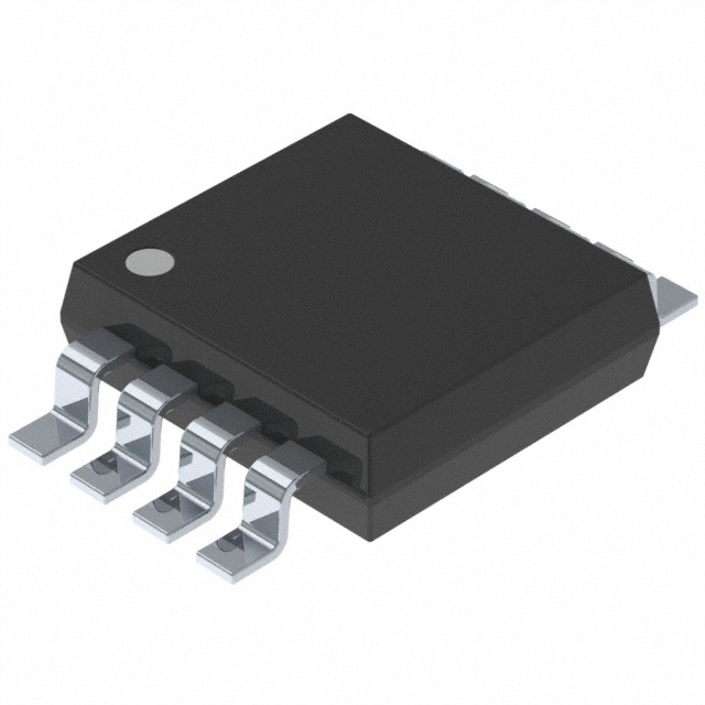
PI6ULS5V9617A
Level Translating Fast-Mode Plus I2C-bus/SMbus Repeater
Features
Description
2-channel, bidirectional buffer isolates capacitance and
The PI6ULS5V9617A is a CMOS integrated circuit intended
for Fast-mode Plus (Fm+) I2C-bus or SMBus applications. It
provides level shifting between low voltage (down to 0.6V)
and higher voltage (2.2V to 5.5V) in mixed-mode applications.
The PI6ULS5V9617A enables the system designer to isolate
two halves of a bus for both voltage and capacitance,
accommodating more I2C devices or longer trace length. It
also permits extension of the I2C-bus by providing
bidirectional buffering for both the data (SDA) and the clock
(SCL) lines, thus enabling two buses of 540 pF at 1 MHz or up
to 4000 pF at lower speeds. The SDA and SCL pins are overvoltage tolerant and are high-impedance when the
PI6ULS5V9617A is un-powered.
The 2.2V to 5.5V bus port B drivers have the static level offset,
while the adjustable voltage bus port A drivers eliminate the
static offset voltage. This results in a LOW on the port B
translating into a nearly 0V LOW on the port A which
accommodates the smaller voltage swings of lower voltage
logic. The EN pin is referenced to VCC(B) and can also be used
to turn the drivers on and off under system control.
allows 540pF on either side of the device at 1 MHz and up
to 4000 pF at lower speeds
Voltage level translation from 0.6V to 5.5V and from 2.2V
to 5.5V
Footprint and functional replacement for PI6ULS5V9617A
at Fast-mode speeds
Port A operating supply voltage range of 0.6V to 5.5V with
normal levels(0.4VCC(A) + 0.8V ≤ VCC(B) )
Port B operating supply voltage range of 2.2V to 5.5V with
static offset level
5V tolerant I2C-bus and enable pins
0 Hz to 1 MHz clock frequency (the maximum system
operating frequency may be less than 1MHz because of the
delays added by the repeater)
Active HIGH repeater enable input referenced to VCC(B)
Open-drain input/outputs
Latching free operation
Supports arbitration and clock stretching across the
repeater
Accommodates Standard-mode, Fast-mode and Fast-mode
Plus I2C-bus devices, SMBus (standard and high power
mode), PMBus and multiple masters
Powered-off high-impedance I2C-bus pins
ESD protection exceeds 8000V HBM per JESD22-A114
Totally Lead-Free & Fully RoHS Compliant (Notes 1 & 2)
Halogen and Antimony Free. “Green” Device (Note 3)
For automotive applications requiring specific change
control (i.e. parts qualified to AEC-Q100/101/200, PPAP
capable, and manufactured in IATF 16949 certified
facilities), please contact us or your local Diodes
representative.
Block Diagram
https://www.diodes.com/quality/product-definitions/
Packaging (Pb-free & Green):
。 MSOP-8(U)
。 SOIC-8(W)
。 TDFN-8(ZE)
EN
H
L
Function
SCLA = SCLB;
SDAA = SDAB;
disabled
Notes:
1. No purposely added lead. Fully EU Directive 2002/95/EC (RoHS), 2011/65/EU (RoHS 2) & 2015/863/EU (RoHS 3) compliant.
2. See https://www.diodes.com/quality/lead-free/ for more information about Diodes Incorporated’s definitions of Halogen- and Antimony-free, "Green" and Lead-free.
3. Halogen- and Antimony-free "Green” products are defined as those which contain
很抱歉,暂时无法提供与“PI6ULS5V9617AUE”相匹配的价格&库存,您可以联系我们找货
免费人工找货