PI74AVC+16245
12345678901234567890123456789012123456789012345678901234567890121234567890123456789012345678901212345678901234567890123456789012123456789012
12345678901234567890123456789012123456789012345678901234567890121234567890123456789012345678901212345678901234567890123456789012123456789012
2.5V 16-Bit Bidirectional Transceiver
with 3-State Outputs
Product Features
Product Description
PI74AVC+16245 is designed for low-voltage operation,
VCC = 1.65V to 3.6V
Pericom Semiconductors PI74AVC+ series of logic circuits are
produced using the Companys advanced submicron CMOS
technology, achieving industry leading speed.
True ±24mA Balanced Drive @ 3.3V
The PI74AVC+16245 is a 16-bit bidirectional transceiver designed
for asynchronous two-way communication between data buses.
The direction control input pin (xDIR) determines the direction of
data flow through the bidirectional transceiver. The Direction and
Output Enable controls are designed to operate this device as either
two independent 8-bit transceivers or one 16-bit transceiver. The
output enable (OE) input, when HIGH, disables both A and B ports
by placing them in HIGH Z condition.
To ensure the high-impedance state during power up or power
down, OE should be tied to VCC through a pull-up resistor; the
minimum value of the resistor is determined by the current sinking
ability of the driver.
Compatible with Philips and T.I. AVC Logic family
IOFF supports partial power-down operation
3.6V I/O Tolerant inputs and outputs
All outputs contain a patented DDC
(Dynamic Drive Control) circuit that reduces noise
without degrading propagation delay
Industrial operation: 40°C to +85°C
Available Packages:
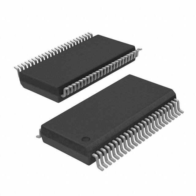
48-pin 240-mil wide plastic TSSOP
48-pin 173-mil wide plastic TVSOP
Logic Block Diagram
1DIR
2DIR
1OE
2OE
1A0
2A0
1B0
2B0
1A1
2A1
1B1
2B1
1A2
2A2
1B2
2B2
1A3
2A3
1B3
2B3
1A4
2A4
1B4
2B4
1A5
2A5
1B5
2B5
1A6
2A6
1B6
2B6
1A7
2A7
1B7
2B7
1
PS8524
12/10/01
�PI74AVC+16245
2.5V 16-Bit Bidirectional
Transceiver with 3-State Outputs
12345678901234567890123456789012123456789012345678901234567890121234567890123456789012345678901212345678901234567890123456789012123456789012
12345678901234567890123456789012123456789012345678901234567890121234567890123456789012345678901212345678901234567890123456789012123456789012
Maximum Ratings (Above which the useful life may be impaired. For user guidelines, not tested.)
Notes:
Stresses greater than those listed under MAXIMUM
RATINGS may cause permanent damage to the device.
This is a stress rating only and functional operation of the device
at these or any other conditions above those indicated in the
operational sections of this specification is not implied. Exposure
to absolute maximum rating conditions for extended periods may
affect reliability.
Supply voltage range, VCC .............................. 0.5V to +4.6V
Input voltage range, VI ....................................0.5V to +4.6V
Voltage range applied to any output in the
high-impedance or power-off state, VO(1) ........0.5V to +4.6V
Voltage range applied to any output in the
high or low state, VO(1,2) ........................... 0.5V to VCC +0.5V
Input clamp current, IIK (VI < 0) ................................... 50mA
Output clamp current, IOK (VO < 0) .............................. 50mA
Continuous output current, IO .................................... ±50mA
Continuous current through each VCC or GND .......... ±100mA
Package thermal impedance, θJA(3): package A .......... 64°C/W
package K ......... 48°C/W
Storage Temperature range, Tstg ......................65°C to 150°C
1. Input & output negative-voltage ratings may be
exceeded if the input and output curent rating are observed.
2. Output positive-voltage rating may be exceeded up to 4.6V
maximum if the output current rating is observed.
3. The package thermal impedance is calculated in accordance with
JESD 51.
Product Pin Configuration
Product Pin Description
Pin Name
De s cription
1DIR
1
48
1OE
xO E
3- State Output Enable Inputs (Active LOW)
1B0
2
47
1A0
1B1
3
46
1A1
xDIR
Direction Control Input
GND
4
45
GND
XAX
Side A Inputs or 3- State Inputs
1B2
5
44
1A2
XBX
Side B Outputs or 3- State Outputs
1B3
6
43
1A3
VCC
7
42
VCC
GND
Ground
1B4
8
41
1A4
VCC
Power
1B5
9
40
1A5
GND
10
39
GND
1B6
11
38
1A6
1B7
12
37
1A7
2B0
13
36
2A0
2B1
14
35
GND
15
2B2
2B3
48-Pin
A,V
Truth Table(1)
Inputs (1)
Outputs (1)
xOE
xDIR
2A1
L
L
Bus B Data to Bus A
34
GND
L
H
Bus A Data to Bus B
16
33
2B2
17
32
2A3
H
X
Z
VCC
18
31
VCC
2B4
19
30
2A4
2B5
20
29
2A5
GND
21
28
GND
2B6
22
27
2A6
2B7
23
26
2A7
2DIR
24
25
2OE
Notes:
1. H = High Signal Level
L = Low Signal Level
X = Dont Care or Irrelevant
Z = High Impedance
2
PS8524
12/10/01
�PI74AVC+16245
2.5V 16-Bit Bidirectional
Transceiver with 3-State Outputs
12345678901234567890123456789012123456789012345678901234567890121234567890123456789012345678901212345678901234567890123456789012123456789012
12345678901234567890123456789012123456789012345678901234567890121234567890123456789012345678901212345678901234567890123456789012123456789012
Recommended Operating Conditions(1)
VCC
Supply Voltage
M in.
M ax.
Operating
1.4
3.6
Data retention only
1.2
VCC = 1.2V
VIH
High- level Input Voltage
VCC
VCC = 1.4V to 1.6V
0.65 x VCC
VCC = 1.65V to 1.95V
0.65 x VCC
VCC = 2.3V to 2.7V
VCC = 3V to 3.6V
1.7
2
VCC = 1.2V
VIL
Low- level Input Voltage
VI
Input Voltage
VO
Output Voltage
IOHS High- level output current
IOLS
Low- level output current
DtDv Input transition rise or fall rate
TA
Units
V
GND
VCC = 1.4V to 1.6V
0.35 x VCC
VCC = 1.65V to 1.95V
0.35 x VCC
VCC = 2.3V to 2.7V
0.7
VCC = 3V to 3.6V
0.8
0
3.6
Active State
0
VCC
3- State
0
3.6
VCC = 1.4V to 1.6V
4
VCC = 1.65V to 1.95V
6
VCC = 2.3V to 2.7V
12
VCC = 3V to 3.6V
24
mA
VCC = 1.4V to 1.6V
4
VCC = 1.65V to 1.95V
6
VCC = 2.3V to 2.7V
12
VCC = 3V to 3.6V
24
VCC = 1.4V to 3.6V
5
ns/V
85
°C
Operating free- air temperature
40
Notes:
1. All unused inputs must be held at VCC or GND to ensure proper device operation.
3
PS8524
12/10/01
�PI74AVC+16245
2.5V 16-Bit Bidirectional
Transceiver with 3-State Outputs
12345678901234567890123456789012123456789012345678901234567890121234567890123456789012345678901212345678901234567890123456789012123456789012
12345678901234567890123456789012123456789012345678901234567890121234567890123456789012345678901212345678901234567890123456789012123456789012
DC Electrical Characteristics (Over the Operating Range, TA = 40°C +85°C)
Te s t Conditions (1)
Parame te rs
IO H = 100µA
VO H
M in.
1.4V to 3.6V
VC C 0.2V
IO HS = 4mA
VIH = 0.91V
1.4V
1.05
IO HS = 6mA
VIH = 1.07V
1.65V
1.2
IO HS = 12mA
VIH = 1.7V
2.3V
1.75
IO HS = 24mA
VIH = 2V
3V
2.0
IO LS = 100µA
VO L
VCC
M ax.
1.4V to 3.6V
0.2
IO LS = 4mA
VIL = 0.49V
1.4V
0.4
IO LS = 6mA
VIL = 0.57V
1.65V
0.45
IO LS = 12mA
VIL = 0.7V
2.3V
0.55
IO LS = 24mA
VIL = 0.8V
3V
0.8
II
VI = VC C or GND
3.6V
±2.5
IO FF
VI or VO = 3.6V
0
±10
IO Z
VO = VC C or GND
3.6V
±10
IC C
VI = VC C or GND
3.6V
40
IO = 0
Control Inputs
VI = VC C or GND
CI
Data Inputs
CO
Typ.
Outputs
VO = VC C or GND
2.5V
3.5
3.3V
3.5
2.5V
6
3.3V
6
2.5V
6.5
3.3V
6.5
Units
V
µA
pF
Note:
1. Typical values are measured at TA = 25°C.
4
PS8524
12/10/01
�PI74AVC+16245
2.5V 16-Bit Bidirectional
Transceiver with 3-State Outputs
12345678901234567890123456789012123456789012345678901234567890121234567890123456789012345678901212345678901234567890123456789012123456789012
12345678901234567890123456789012123456789012345678901234567890121234567890123456789012345678901212345678901234567890123456789012123456789012
Switching Characteristics
(Over recommended operating free-air temperature range, unless otherwise noted, see Figures 1 thru 4)
VCC = 1.5V
± 0.1V
From
(Input)
To
(Output)
VCC = 1.2V
Typ.
M in.
tpd
A
Y
3.9
0.8
4.0
ten
OE
Y
8.4
1.5
tdis
OE
Y
8.4
2.3
Parame te rs
VCC = 1.8V
± 0.15V
M ax. M in.
VCC = 2.5V
± 0.2V
VCC = 3.3V
± 0.3V
M ax.
M in.
M ax.
M in.
M ax.
0.7
3.0
0.6
1.9
0.5
1.7
9.2
1.4
7.0
1.0
4.3
0.7
3.7
9.3
2.2
7.0
1.1
4.0
1.2
3.9
Units
ns
Operating Characteristics, TA= 25°C
Parame te rs
Cpd Power Dissipation
Capacitance
Te s t Conditions
O utputs Enabled
O utputs Disabled
CL = 0pF,
f = 10 MHz
5
VCC = 1.8V
±0.15V
VCC = 2.5V
±0.2V
VCC = 3.3V
±0.3V
Typical
Typical
Typical
35
38
44
6
6
7
Units
pF
PS8524
12/10/01
�PI74AVC+16245
2.5V 16-Bit Bidirectional
Transceiver with 3-State Outputs
12345678901234567890123456789012123456789012345678901234567890121234567890123456789012345678901212345678901234567890123456789012123456789012
12345678901234567890123456789012123456789012345678901234567890121234567890123456789012345678901212345678901234567890123456789012123456789012
PARAMETER MEASUREMENT INFORMATION
VCC = 1.2V and 1.5V ± 0.1V
2xVCC
S1
2Ω
From Output
Under Test
CL = 15pF
Open
GND
2Ω
(See Note A)
Te s t
S1
tpd
tPLZ/tPZL
tPHZ/tPZH
Open
2 x VCC
GND
Load Circuit
VCC
Timing
Input
VCC/2
tW
0V
tsu
VCC
VCC/2
Input
th
VCC/2
0V
VCC
Data
Input
VCC/2
VCC/2
Voltage Waveforms
Pulse Duration
0V
Voltage Waveforms
Setup and Hold Times
Output
Control
(Low Level
Enabling)
VCC
Input
VCC/2
VCC/2
tPLH
tPHL
VOH
Output
VCC/2
Output
Waveform 2
S1 at GND
(see Note B)
VCC/2
VOL
Voltage Waveforms
Propagation Delay Times
VCC/2
0V
tPZL
Output
Waveform 1
S1 at 2 x VCC
(see Note B) t
PZH
0V
VCC /2
VCC
tPLZ
VCC
VCC/2
VOL +0.1V
VOL
tPHZ
VCC/2
VOH –0.1V
VOH
0V
Voltage Waveforms
Enable and Disable Times
Figure 1. Load Circuit and Voltage Waveforms
Notes:
A. CL includes probe and jig capacitance.
B. Waveform 1 is for an output with internal conditions such that the output is low except when disabled by the output control.
Waveform 2 is for an output with internal conditions such that the output is high except when disabled by the output control.
C. All input impulses are supplied by generators having the following characteristics: PRR ≤ 10 MHz, ZO = 50Ω, tR ≤ 2.0ns, tF ≤ 2.0ns.
D. The outputs are measured one at a time with one transition per measurement.
E. tPLZ and tPHZ are the same as tdis
F. tPZL and tPZH are the same as ten
G. tPLH and tPHL are the same as tpd
6
PS8524
12/10/01
�PI74AVC+16245
2.5V 16-Bit Bidirectional
Transceiver with 3-State Outputs
12345678901234567890123456789012123456789012345678901234567890121234567890123456789012345678901212345678901234567890123456789012123456789012
12345678901234567890123456789012123456789012345678901234567890121234567890123456789012345678901212345678901234567890123456789012123456789012
PARAMETER MEASUREMENT INFORMATION
VCC = 1.8V ±0.15V
2xVCC
S1
12ΩkΩ
From Output
Under Test
CL = 30
15pF
Open
GND
2Ω
1 kΩ
(See Note A)
Te s t
S1
tpd
tPLZ/tPZL
tPHZ/tPZH
Open
2 x VCC
GND
Load Circuit
VCC
Timing
Input
VCC/2
tW
0V
tsu
VCC
VCC/2
Input
th
VCC/2
0V
VCC
Data
Input
VCC/2
VCC/2
Voltage Waveforms
Pulse Duration
0V
Voltage Waveforms
Setup and Hold Times
Output
Control
(Low Level
Enabling)
VCC
Input
VCC/2
VCC/2
tPLH
tPHL
VOH
Output
VCC/2
Output
Waveform 2
S1 at GND
(see Note B)
VCC/2
VOL
Voltage Waveforms
Propagation Delay Times
VCC/2
0V
tPZL
Output
Waveform 1
S1 at 2 x VCC
(see Note B) t
PZH
0V
VCC /2
VCC
tPLZ
VCC
VCC/2
VOL +0.1V
0.15V
VOL
tPHZ
VCC/2
VOH –0.1V
0.15V
VOH
0V
Voltage Waveforms
Enable and Disable Times
Figure 2. Load Circuit and Voltage Waveforms
Notes:
A. CL includes probe and jig capacitance.
B. Waveform 1 is for an output with internal conditions such that the output is low except when disabled by the output control.
Waveform 2 is for an output with internal conditions such that the output is high except when disabled by the output control.
C. All input impulses are supplied by generators having the following characteristics: PRR ≤ 10 MHz, ZO = 50Ω, tR ≤ 2.0ns, tF ≤ 2.0ns.
D. The outputs are measured one at a time with one transition per measurement.
E. tPLZ and tPHZ are the same as tdis
F. tPZL and tPZH are the same as ten
G. tPLH and tPHL are the same as tpd
7
PS8524
12/10/01
�PI74AVC+16245
2.5V 16-Bit Bidirectional
Transceiver with 3-State Outputs
12345678901234567890123456789012123456789012345678901234567890121234567890123456789012345678901212345678901234567890123456789012123456789012
12345678901234567890123456789012123456789012345678901234567890121234567890123456789012345678901212345678901234567890123456789012123456789012
PARAMETER MEASUREMENT INFORMATION
VCC = 2.5V ±0.2V
2xVCC
S1
500Ω
2Ω
From Output
Under Test
CL =30
15pF
Open
GND
500Ω
2Ω
(See Note A)
Te s t
S1
tpd
tPLZ/tPZL
tPHZ/tPZH
Open
2 x VCC
GND
Load Circuit
VCC
Timing
Input
VCC/2
tW
0V
tsu
VCC
VCC/2
Input
th
VCC/2
0V
VCC
Data
Input
VCC/2
VCC/2
Voltage Waveforms
Pulse Duration
0V
Voltage Waveforms
Setup and Hold Times
Output
Control
(Low Level
Enabling)
VCC
Input
VCC/2
VCC/2
tPLH
tPHL
VOH
Output
VCC/2
Output
Waveform 2
S1 at GND
(see Note B)
VCC/2
VOL
Voltage Waveforms
Propagation Delay Times
VCC/2
0V
tPZL
Output
Waveform 1
S1 at 2 x VCC
(see Note B) t
PZH
0V
VCC /2
VCC
tPLZ
VCC
VCC/2
VOL +0.15V
VOL
tPHZ
VCC/2
VOH –0.15V
VOH
0V
Voltage Waveforms
Enable and Disable Times
Figure 3. Load Circuit and Voltage Waveforms
Notes:
A. CL includes probe and jig capacitance.
B. Waveform 1 is for an output with internal conditions such that the output is low except when disabled by the output control.
Waveform 2 is for an output with internal conditions such that the output is high except when disabled by the output control.
C. All input impulses are supplied by generators having the following characteristics: PRR ≤ 10 MHz, ZO = 50Ω, tR ≤ 2.0ns, tF ≤ 2.0ns.
D. The outputs are measured one at a time with one transition per measurement.
E. tPLZ and tPHZ are the same as tdis
F. tPZL and tPZH are the same as ten
G. tPLH and tPHL are the same as tpd
8
PS8524
12/10/01
�PI74AVC+16245
2.5V 16-Bit Bidirectional
Transceiver with 3-State Outputs
12345678901234567890123456789012123456789012345678901234567890121234567890123456789012345678901212345678901234567890123456789012123456789012
12345678901234567890123456789012123456789012345678901234567890121234567890123456789012345678901212345678901234567890123456789012123456789012
PARAMETER MEASUREMENT INFORMATION
VCC = 3.3V ±0.3V
2xVCC
S1
500Ω
2Ω
From Output
Under Test
CL = 30
15pF
Open
GND
500Ω
2Ω
(See Note A)
Te s t
S1
tpd
tPLZ/tPZL
tPHZ/tPZH
Open
2 x VCC
GND
Load Circuit
VCC
Timing
Input
VCC/2
tW
0V
tsu
VCC
VCC/2
Input
th
VCC/2
0V
VCC
Data
Input
VCC/2
VCC/2
Voltage Waveforms
Pulse Duration
0V
Voltage Waveforms
Setup and Hold Times
Output
Control
(Low Level
Enabling)
VCC
Input
VCC/2
VCC/2
tPLH
tPHL
VOH
Output
VCC/2
Output
Waveform 2
S1 at GND
(see Note B)
VCC/2
VOL
Voltage Waveforms
Propagation Delay Times
VCC/2
0V
tPZL
Output
Waveform 1
S1 at 2 x VCC
(see Note B) t
PZH
0V
VCC /2
VCC
tPLZ
VCC
VCC/2
VOL +0.1V
0.3V
VOL
tPHZ
VCC/2
VOH –0.1V
0.3V
VOH
0V
Voltage Waveforms
Enable and Disable Times
Figure 4. Load Circuit and Voltage Waveforms
Notes:
A. CL includes probe and jig capacitance.
B. Waveform 1 is for an output with internal conditions such that the output is low except when disabled by the output control.
Waveform 2 is for an output with internal conditions such that the output is high except when disabled by the output control.
C. All input impulses are supplied by generators having the following characteristics: PRR ≤ 10 MHz, ZO = 50Ω, tR ≤ 2.0ns, tF ≤ 2.0ns.
D. The outputs are measured one at a time with one transition per measurement.
E. tPLZ and tPHZ are the same as tdis
F. tPZL and tPZH are the same as ten
G. tPLH and tPHL are the same as tpd
9
PS8524
12/10/01
�PI74AVC+16245
2.5V 16-Bit Bidirectional
Transceiver with 3-State Outputs
12345678901234567890123456789012123456789012345678901234567890121234567890123456789012345678901212345678901234567890123456789012123456789012
12345678901234567890123456789012123456789012345678901234567890121234567890123456789012345678901212345678901234567890123456789012123456789012
Packaging Mechanical - 48-pin TSSOP (A-package)
48
.236
.244
1
6.0
6.2
.488 12.4
.496 12.6
.047
1.20 Max
SEATING PLANE
.004 0.09
.008 0.20
X.XX
X.XX
DENOTES DIMENSIONS
IN MILLIMETERS
.0197
BSC
0.50
0.45 .018
0.75 .030
.002
.006
0.05
0.15
.007
.010
0.17
0.27
.319
BSC
8.1
Packaging Mechanical - 48-pin TVSOP (TSSOP) (K-package)
48
.169
.177
4.30
4.50
.0035
.008
.031
.041
0.80
1.05
1
.378 9.60
.386 9.80
0.09
0.20
0.45 .018
0.75 .030
.252
BSC
6.4
SEATING
PLANE
X.XX DENOTES DIMENSIONS
X.XX IN MILLIMETERS
.016
BSC
0.40
.002
.006
0.05
0.15
.0051
.009
0.13
0.23
Max.
.047
1.20
Ordering Information
Orde ring Code
D e s cription
PI74AVC+16245A
48- pin, 240- mil wide plastic TSSO P
PI74AVC+16245K
48- pin, 173- mil wide plastic TVSO P
Pericom Semiconductor Corporation
2380 Bering Drive San Jose, CA 95131 1-800-435-2336 Fax (408) 435-1100 http://www.pericom.com
10
PS8524
12/10/01
�
很抱歉,暂时无法提供与“PI74AVC+16245A”相匹配的价格&库存,您可以联系我们找货
免费人工找货