PI74LPT573
12345678901234567890123456789012123456789012345678901234567890121234567890123456789012345678901212345678901234567890123456789012123456789012
12345678901234567890123456789012123456789012345678901234567890121234567890123456789012345678901212345678901234567890123456789012123456789012
Fast CMOS 3.3V 8-Bit
Transparent Latch
Features
Description
• Compatible with LCX™ and LVT™ families of products
• Supports 5V Tolerant Mixed Signal Mode Operation
– Input can be 3V or 5V
– Output can be 3V or connected to 5V bus
• Advanced Low Power CMOS Operation
• Excellent output drive capability:
Balanced drives (24 mA sink and source)
• Low ground bounce outputs
• Hysteresis on all inputs
• Industrial operating temperature range: –40°C to +85°C
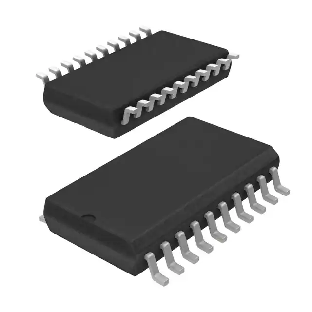
• Packages available:
– 20-pin 173 mil wide plastic TSSOP (L)
– 20-pin 150 mil wide plastic QSOP (Q)
– 20-pin 150 mil wide plastic TQSOP (R)
– 20-pin 300 mil wide plastic SOIC (S)
Pericom Semiconductor’s PI74LPT series of logic circuits are produced in the Company’s advanced 0.6 micron CMOS technology,
achieving industry leading speed grades.
Logic Block Diagram
Pinout
The PI74LPT573 is an 8-bit transparent latch designed with
3-state outputs and is intended for bus oriented applications. When
Latch Enable (LE) is HIGH, the flip-flops appear transparent to the
data. The data that meets the set-up time when LE is LOW is latched.
When OE is HIGH, the bus output is in the high impedance state.
The PI74LPT573 can be driven from either 3.3V or 5.0V devices
allowing this device to be used as a translator in a mixed
3.3/5.0V system.
OE
OE
D0
D1
D2
D3
D4
D5
D6
D7
GND
LE
D0
D
O0
O
G
20
1
19
2
18
3
20-Pin
17
4
L20 16
5
R20
15
6
Q20
7
S20 14
13
8
12
9
11
10
Vcc
O0
O1
O2
O3
O4
O5
O6
O7
LE
TO 7 OTHER CHANNELS
Truth Table
Pin Description
(1)
DN
H
L
X
Inputs
LE
H
H
X
(1)
OE
L
L
H
Outputs
ON
H
L
Z
Pin Name
OE
LE
D7-D0
O7-O0
GND
VCC
Note:
1. H = High Voltage Level, X = Don't Care,
L = Low Voltage Level, Z = High Impedance
1
Description
Output Enable Input (Active LOW)
Latch Enable Input (Active HIGH)
Data Inputs
3-State Outputs
Ground
Power
PS2063A 01/15/97
�PI74LPT573
3.3V
8-BIT
TRANSPARENT
LATCH
12345678901234567890123456789012123456789012345678901234567890121234567890123456789012345678901212345678901234567890123456789012123456789012
Maximum Ratings
(Above which the useful life may be impaired. For user guidelines, not tested.)
Storage Temperature ............................................................. –65°C to +150°C
Ambient Temperature with Power Applied ............................ –40°C to +85°C
Supply Voltage to Ground Potential (Inputs & Vcc Only) ...... –0.5V to +7.0V
Supply Voltage to Ground Potential (Outputs & D/O Only) .. –0.5V to +7.0V
DC Input Voltage .................................................................... –0.5V to +7.0V
DC Output Current .............................................................................. 120 mA
Power Dissipation .................................................................................... 1.0W
Note:
Stresses greater than those listed under MAXIMUM
RATINGS may cause permanent damage to the device. This is a stress rating only and functional operation of the device at these or any other conditions
above those indicated in the operational sections of
this specification is not implied. Exposure to absolute
maximum rating conditions for extended periods may
affect reliability.
DC Electrical Characteristics (Over the Operating Range, TA = –40°C to +85°C, VCC = 2.7V to 3.6V)
Parameters
IOZH
IOZL
VIK
IODH
IODL
VOH
Input HIGH Voltage (Input pins)
Input HIGH Voltage (I/O pins)
Input LOW Voltage
(Input and I/O pins)
Input HIGH Current (Input pins)
Input HIGH Current (I/O pins)
Input LOW Current (Input pins)
Input LOW Current (I/O pins)
High Impedance Output Current
(3-State Output pins)
Clamp Diode Voltage
Output HIGH Current
Output LOW Current
Output HIGH Voltage
VOL
Output LOW Voltage
IOS
IOFF
VH
Short Circuit Current(4)
Power Down Disable
Input Hysteresis
VIH
VIL
IIH
IIL
Test Conditions(1)
Description
Guaranteed Logic HIGH Level
Guaranteed Logic LOW Level
Min.
Typ(2)
Max.
Units
2.2
2.0
–0.5
—
—
—
5.5
5.5
0.8
V
V
V
—
—
—
—
—
—
–0.7
–60
90
—
3.0
3.0
—
—
0.2
0.3
–85
—
150
±1
±1
±1
±1
±1
±1
–1.2
–110
200
—
—
—
—
0.2
0.4
0.5
–240
±100
—
µA
µA
µA
µA
µA
µA
V
mA
mA
V
V
V
VCC = Max.
VIN = 5.5V
—
VCC = Max.
VIN = VCC
—
VCC = Max.
VIN = GND
—
VCC = Max.
VIN = GND
—
VCC = Max.
VOUT = 5.5V
—
VCC = Max.
VOUT = GND
—
VCC = Min., IIN = –18 mA
—
VCC = 3.3V, VIN = VIH or VIL, VO = 1.5V(3)
–36
VCC = 3.3V, VIN = VIH or VIL, VO = 1.5V(3)
50
VCC = Min.
IOH = –0.1 mA Vcc-0.2
VIN = VIH or VIL
IOH = –3 mA
2.4
VCC = 3.0V,
IOH = –8 mA
2.4(5)
VIN = VIH or VIL
IOH = –24 mA
2.0
VCC = Min.
IOL = 0.1 mA
—
VIN = VIH or VIL
IOL = 16 mA
—
IOL = 24 mA
—
VCC = Max.(3), VOUT = GND
–60
VCC = 0V, VIN or VOUT ≤ 4.5V
—
—
V
V
V
mA
µA
mV
Notes:
1. For Max. or Min. conditions, use appropriate value specified under Electrical Characteristics for the applicable device type.
2. Typical values are at Vcc = 3.3V, +25°C ambient and maximum loading.
3. Not more than one output should be shorted at one time. Duration of the test should not exceed one second.
4. This parameter is guaranteed but not tested.
5. VOH = VCC – 0.6V at rated current.
Capacitance (TA = 25°C, f = 1 MHz)
Parameters(1)
CIN
COUT
Description
Test Conditions
Input Capacitance
Output Capacitance
VIN = 0V
VOUT = 0V
Typ.
Max.
Units
4.5
5.5
6
8
pF
pF
Note:
1. This parameter is determined by device characterization but is not production tested.
2
PS2063A 01/15/97
�PI74LPT573
3.3V
8-BIT
TRANSPARENT
LATCH
12345678901234567890123456789012123456789012345678901234567890121234567890123456789012345678901212345678901234567890123456789012123456789012
Power Supply Characteristics
Parameters Description
Test Conditions(1)
Min.
Typ(2)
Max.
Units
ICC
Quiescent Power Supply Current
VCC = Max.
VIN = GND or VCC
0.1
10
µA
∆ICC
Quiescent Power Supply Current
TTL Inputs HIGH
VCC = Max.
VIN = VCC – 0.6V(3)
2.0
30
µA
ICCD
Dynamic Power Supply(4)
VCC = Max.,
Outputs Open
OE = GND
One Bit Toggling
50% Duty Cycle
VIN = VCC
VIN = GND
50
75
µA/
MHz
VCC = Max.,
Outputs Open
fI = 10 MHZ
50% Duty Cycle
OE = GND
One Bit Toggling
VIN = VCC – 0.6V
VIN = GND
0.6
VCC = Max.,
Outputs Open
fI = 2.5 MHZ
50% Duty Cycle
OE = GND
8 Bits Toggling
VIN = VCC – 0.6V
VIN = GND
IC
Total Power Supply
Current(6)
2.3
mA
1
2
3
4
5
2.1
4.7(5)
6
7
Notes:
1. For Max. or Min. conditions, use appropriate value specified under Electrical Characteristics for the applicable device.
2. Typical values are at Vcc = 3.3V, +25°C ambient.
3. Per TTL driven input; all other inputs at Vcc or GND.
4. This parameter is not directly testable, but is derived for use in Total Power Supply Calculations.
5. Values for these conditions are examples of the Icc formula. These limits are guaranteed but not tested.
6. IC =IQUIESCENT + IINPUTS + IDYNAMIC
IC = ICC + ∆ICC DHNT + ICCD (fCP/2 + fINI)
ICC = Quiescent Current (ICCL, ICCH and ICCZ)
∆ICC = Power Supply Current for a TTL High Input
DH = Duty Cycle for TTL Inputs High
NT = Number of TTL Inputs at DH
ICCD = Dynamic Current Caused by an Input Transition Pair (HLH or LHL)
fCP = Clock Frequency for Register Devices (Zero for Non-Register Devices)
NCP = Number of Clock Inputs at fCP
fI = Input Frequency
NI = Number of Inputs at fI
All currents are in milliamps and all frequencies are in megahertz.
8
9
10
11
12
13
14
15
3
PS2063A 01/15/97
�PI74LPT573
3.3V
8-BIT
TRANSPARENT
LATCH
12345678901234567890123456789012123456789012345678901234567890121234567890123456789012345678901212345678901234567890123456789012123456789012
Switching Characteristics over Operating Range(1)
LPT573
LPT573A
Com.
Parameters
(2)
3)
LPT573C
Com.
Com.
Max.
Min.
(3)
Description
Conditions
Min.
Max.
tPLH
tPHL
Propagation Delay
Dx to Ox
CL = 50pF
RL = 500Ω
1.5
8.0
1.5
5.2
tPLH
tPHL
Propagation Delay
LE to Ox
2.0
12.0
2.0
tPZH
tPZL
Output Enable Time
OE to Ox
1.5
9.5
tPHZ
tPLZ
Output Disable Time(4)
OE to Ox
1.5
6.5
tSU
Setup Time HIGH
or LOW, Dx to LE
2.0
2.0
2.0
ns
tH
Hold Time HIGH
or LOW, Dx to LE
1.5
1.5
1.5
ns
tW
LE Pulse Width(4)
HIGH
6.0
5.0
5.0
ns
tSK(o)
Output Skew(5)
0.5
Min.
(3)
Max.
Units
1.5
4.2
ns
8.5
2.0
5.5
ns
1.5
6.5
1.5
5.5
ns
1.5
5.5
1.5
5.0
ns
0.5
0.5
ns
Notes:
1. Propagation Delays and Enable/Disable times are with Vcc = 3.3V ±0.3V, normal range. For Vcc = 2.7V,
extended range, all Propagation Delays and Enable/Disable times should be degraded by 20%.
2. See test circuit and waveforms.
3. Minimum limits are guaranteed but not tested on Propagation Delays.
4. This parameter is guaranteed but not production tested.
5. Skew between any two outputs, of the same package, switching in the same direction.
This parameter is guaranteed by design.
Pericom Semiconductor Corporation
2380 Bering Drive • San Jose, CA 95131 • 1-800-435-2336 • Fax (408) 435-1100 • http://www.pericom.com
4
PS2063A 01/15/97
�
很抱歉,暂时无法提供与“PI74LPT573AS”相匹配的价格&库存,您可以联系我们找货
免费人工找货