PI74STX2G4245
2-Bit Level Shifting Buffer/Transceiver
with Configurable Dual Supply Voltage
Features
Description
• Operation Voltage: 1.65V ≤ VDDA ≤ 3.6V
2.3V ≤ VDDB ≤ 5.5V
VDDA ≤ VDDB
Pericom Semiconductor’s PI74STX2G4245, a 2-bit noninverting
buffer/transceiver, contains two separate supply rails:A port
(VDDA), set to operate from 1.8V to 3.3V; B port (VDDB), set
to operate from 2.5V to 5V. The A1 to B1 translation is configured as an unidirectional buffer; the translation between
A2 and B2 is bidirectional and its direction is controlled
by the DIR pin. The DIR pin is supplied by VDDB.
• High Speed: tpd = 5ns typical into 30pF @ 3V VDD
• Power down high-impedance inputs and outputs
• High output drive: ±12mA at 3V VDDA/VDDB
±24mA at 5V VDDB
• Industrial operation at –40°C to +85°C
• Packaging (Pb-free & Green available):
– 8-pin MSOP (U)
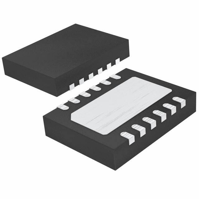
– 12-pin TDFN (ZE)
Block Diagram
DIR
A2
Pin Configuration (MSOP)
4
3
6
A1
2
(1.8V to 3.3V)VDDA
1
8
A1
2
7
B1
A2
3
6
B2
DIR
4
5
GND
VDDB (2.5V to 5V)
B2
7
B1
Pin Configuration (TDFN)
Function Table
Input
Output
DIR
DATA
L
B2
A2
H
A2
B2
NC
1
12
NC
B1
(1.8V to 3.3V ) VDDA
2
11
VDDB (2.5V to 5V)
A1
3
10
B1
A2
4
9
B2
X
A1
Pin Description
Pin Name
Description
DIR
5
8
GND
DIR
Direction Control
NC
6
7
NC
A1
Data Input
B1
Data Output
A2, B2
Data Input/Output
VDDA, VDDB
Power Supply
08-0291
* NC = No Connect
1
PS8729F
10/11/08
�PI74STX2G4245
2-Bit Level Shifting Buffer/Transceiver with
Configurable Dual Supply Voltage
Maximum Ratings
(Absolute maximum ratings over operating free-air temperature range from VDDB at 2.5V & VDDA at 1.2V, unless otherwise noted)
Supply voltage range: VDDA ............................. –0.5V to +6V
VDDB ............................. –0.5V to +6V
Input Voltage Range, VI:
Input A1(1) ................... –0.5V to +6V
I/O A2(1,2) ....... –0.5V to VDDA+0.5V
I/O B2(1,2) ........–0.5V to VDDB+0.5V
Output Voltage Range, VO
Output B1(1,2) ...–0.5V to VDDB +0.5V
DC Input Diode Current, IIK (VO
很抱歉,暂时无法提供与“PI74STX2G4245ZEEX”相匹配的价格&库存,您可以联系我们找货
免费人工找货