PI7C9X2G304EL
PCI EXPRESS GEN 2 PACKET SWITCH
3-Port, 4-Lane, ExtremeLo PCIe2.0 Packet Switch
DATASHEET
REVISION 3
August 2022
1545 Barber Lane Milpitas, CA 95035
Telephone: 408-232-9100
FAX: 408-434-1040
Internet: http://www.diodes.com
Document Number DS39931 Rev 3-2
�PI7C9X2G304EL
IMPORTANT NOTICE
1.
DIODES INCORPORATED (Diodes) AND ITS SUBSIDIARIES MAKE NO WARRANTY OF ANY KIND, EXPRESS OR IMPLIED,
WITH REGARDS TO ANY INFORMATION CONTAINED IN THIS DOCUMENT, INCLUDING, BUT NOT LIMITED TO, THE IMPLIED
WARRANTIES OF MERCHANTABILITY, FITNESS FOR A PARTICULAR PURPOSE OR NON-INFRINGEMENT OF THIRD PARTY
INTELLECTUAL PROPERTY RIGHTS (AND THEIR EQUIVALENTS UNDER THE LAWS OF ANY JURISDICTION).
2.
The Information contained herein is for informational purpose only and is provided only to illustrate the operation of Diodes’ products
described herein and application examples. Diodes does not assume any liability arising out of the application or use of this document or any
product described herein. This document is intended for skilled and technically trained engineering customers and users who design with
Diodes’ products. Diodes’ products may be used to facilitate safety-related applications; however, in all instances customers and users are
responsible for (a) selecting the appropriate Diodes products for their applications, (b) evaluating the suitability of Diodes’ products for their
intended applications, (c) ensuring their applications, which incorporate Diodes’ products, comply the applicable legal and regulatory
requirements as well as safety and functional-safety related standards, and (d) ensuring they design with appropriate safeguards (including
testing, validation, quality control techniques, redundancy, malfunction prevention, and appropriate treatment for aging degradation) to
minimize the risks associated with their applications.
3.
Diodes assumes no liability for any application-related information, support, assistance or feedback that may be provided by Diodes
from time to time. Any customer or user of this document or products described herein will assume all risks and liabilities associated with such
use, and will hold Diodes and all companies whose products are represented herein or on Diodes’ websites, harmless against all damages
and liabilities.
4.
Products described herein may be covered by one or more United States, international or foreign patents and pending patent
applications. Product names and markings noted herein may also be covered by one or more United States, international or foreign
trademarks and trademark applications. Diodes does not convey any license under any of its intellectual property rights or the rights of any
third parties (including third parties whose products and services may be described in this document or on Diodes’ website) under this
document.
5.
Diodes’
products
are
provided
subject
to
Diodes’
Standard
Terms
and
Conditions
of
Sale
(https://www.diodes.com/about/company/terms-and-conditions/terms-and-conditions-of-sales/) or other applicable terms. This document does
not alter or expand the applicable warranties provided by Diodes. Diodes does not warrant or accept any liability whatsoever in respect of any
products purchased through unauthorized sales channel.
6.
Diodes’ products and technology may not be used for or incorporated into any products or systems whose manufacture, use or sale
is prohibited under any applicable laws and regulations. Should customers or users use Diodes’ products in contravention of any applicable
laws or regulations, or for any unintended or unauthorized application, customers and users will (a) be solely responsible for any damages,
losses or penalties arising in connection therewith or as a result thereof, and (b) indemnify and hold Diodes and its representatives and agents
harmless against any and all claims, damages, expenses, and attorney fees arising out of, directly or indirectly, any claim relating to any
noncompliance with the applicable laws and regulations, as well as any unintended or unauthorized application.
7.
While efforts have been made to ensure the information contained in this document is accurate, complete and current, it may
contain technical inaccuracies, omissions and typographical errors. Diodes does not warrant that information contained in this document is
error-free and Diodes is under no obligation to update or otherwise correct this information. Notwithstanding the foregoing, Diodes reserves
the right to make modifications, enhancements, improvements, corrections or other changes without further notice to this document and any
product described herein. This document is written in English but may be translated into multiple languages for reference. Only the English
version of this document is the final and determinative format released by Diodes.
8.
Any unauthorized copying, modification, distribution, transmission, display or other use of this document (or any portion hereof) is
prohibited. Diodes assumes no responsibility for any losses incurred by the customers or users or any third parties arising from any such
unauthorized use.
9. This Notice may be periodically updated with the most recent version available at https://www.diodes.com/about/company/terms-andconditions/important-notice
DIODES is a trademark of Diodes Incorporated in the United States and other countries.
The Diodes logo is a registered trademark of Diodes Incorporated in the United States and other countries.
© 2022 Diodes Incorporated. All Rights Reserved.
www.diodes.com
PI7C9X2G304EL
Document Number DS39931 Rev 3-2
Page 2 of 89
www.diodes.com
August 2022
© 2022 Copyright Diodes Incorporated. All Rights Reserved.
�PI7C9X2G304EL
REVISION HISTORY
Date
03/13/2014
Revision Number
0.1
07/18/2014
1.0
11/17/2014
1.1
07/16/2015
1.2
09/11/2015
1.3
12/23/2015
1.4
02/26/2016
05/05/2016
1.5
1.6
09/05/2017
2-2
08/10/2022
3
PI7C9X2G304EL
Document Number DS39931 Rev 3-2
Description
Preliminary Datasheet
Updated Section 3 Pin Description
Updated Section 4 Pin Assignments
Updated Section 7.2 Transparent Mode Configuration Registers
Updated Section 8 Clock Scheme
Updated Section 3.1 PCI Express Interface Signals
Updated Section 3.2 Port Configuration Signals
Updated Section 5.1 Physical Layer Circuit
Updated Section 6.1 EEPROM Interface
Updated Section 7.2 Transparent Mode Configuration Registers
Updated Section 8 Clock Scheme
Updated Table 9-1 Instruction Register Codes
Updated Table 9-2 JTAG Device ID Register
Updated Table 9-3 JTAG Boundary Scan Register Definition
Updated Table 11-2 DC Electrical Characteristics
Updated Table 11-1 Absolute Maximum Ratings
Updated Section 3.1 PIN Description
Updated Table 11-1 Absolute Maximum Ratings
Updated Table 11-2 DC Electrical Characteristics
Added Section 11 Power Sequence
Updated Section 3.2 Port Configuration Signals
Updated Section 1 Features
Updated Section 3.2 Port Configuration Signals
Updated Section 5.1 Physical Layer Circuit
Updated Section 6.1.4 Mapping EEPROM Contents to Configuration Registers
Updated Section 7.2 Transparent Mode Configuration Registers
Updated Section 12.1 Absolute Maximum Ratings
Updated Table 12-2 DC Electrical Characteristics
Added Section 12.4 Operating Ambient Temperature
Added Section 12.5 Power Consumption
Revision numbering system changed to whole number
Updated Section 3.1 PCI EXPRESS INTERFACE SIGNALS
Updated Section 7.2.47 SWITCH OPERATION MODE – OFFSET 74h (Downstream Port Only)
Updated Section 7.2.53 XPIP_CSR5 – OFFSET 88h
Updated Section 7.2.70 LINK CONTROL REGISTER – OFFSET D0h
Updated Section 8 Clock Scheme
Added Section 13 Thermal Data
Updated Section 7.2.54 TL_CSR – OFFSET 8Ch
Page 3 of 89
www.diodes.com
August 2022
© 2022 Copyright Diodes Incorporated. All Rights Reserved.
�PI7C9X2G304EL
TABLE OF CONTENTS
1
FEATURES ...................................................................................................................................................................... 9
2
GENERAL DESCRIPTION ......................................................................................................................................... 10
3
PIN DESCRIPTION...................................................................................................................................................... 11
3.1
3.2
3.3
3.4
3.5
4
PIN ASSIGNMENTS .................................................................................................................................................... 15
4.1
5
PCI EXPRESS INTERFACE SIGNALS ................................................................................................................... 11
PORT CONFIGURATION SIGNALS ...................................................................................................................... 12
MISCELLANEOUS SIGNALS................................................................................................................................. 12
JTAG BOUNDARY SCAN SIGNALS ..................................................................................................................... 13
POWER PINS ............................................................................................................................................................ 14
PIN LIST OF 136-PIN AQFN ..................................................................................................................................... 15
FUNCTIONAL DESCRIPTION .................................................................................................................................. 16
5.1
PHYSICAL LAYER CIRCUIT ................................................................................................................................. 16
5.1.1
RECEIVER DETECTION .................................................................................................................................. 16
5.1.2
RECEIVER SIGNAL DETECTION .................................................................................................................... 17
5.1.3
RECEIVER EQUALIZATION ............................................................................................................................ 17
5.1.4
TRANSMITTER SWING..................................................................................................................................... 17
5.1.5
DRIVE AMPLITUDE AND DE-EMPHASIS SETTINGS ................................................................................... 17
5.1.6
DRIVE AMPLITUDE ......................................................................................................................................... 18
5.1.7
DRIVE DE-EMPHASIS ..................................................................................................................................... 19
5.1.8
TRANSMITTER ELECTRICAL IDLE LATENCY .............................................................................................. 19
5.2
DATA LINK LAYER (DLL) ..................................................................................................................................... 19
5.3
TRANSACTION LAYER RECEIVE BLOCK (TLP DECAPSULATION) ............................................................. 20
5.4
ROUTING ................................................................................................................................................................. 20
5.5
TC/VC MAPPING ..................................................................................................................................................... 20
5.6
QUEUE ...................................................................................................................................................................... 20
5.6.1
PH ...................................................................................................................................................................... 21
5.6.2
PD ...................................................................................................................................................................... 21
5.6.3
NPHD ................................................................................................................................................................ 21
5.6.4
CPLH ................................................................................................................................................................. 21
5.6.5
CPLD ................................................................................................................................................................. 21
5.7
TRANSACTION ORDERING .................................................................................................................................. 21
5.8
PORT ARBITRATION ............................................................................................................................................. 22
5.9
VC ARBITRATION .................................................................................................................................................. 22
5.10 FLOW CONTROL .................................................................................................................................................... 22
5.11 TRANSATION LAYER TRANSMIT BLOCK (TLP ENCAPSULATION) ............................................................ 23
5.12 ACCESS CONTROLS SERVICE ............................................................................................................................. 23
6
EEPROM INTERFACE AND SYSTEM MANAGEMENT BUS............................................................................. 24
6.1
EEPROM INTERFACE............................................................................................................................................. 24
6.1.1
AUTO MODE EERPOM ACCESS..................................................................................................................... 24
6.1.2
EEPROM MODE AT RESET ............................................................................................................................. 24
6.1.3
EEPROM SPACE ADDRESS MAP ................................................................................................................... 24
6.1.4
MAPPING EEPROM CONTENTS TO CONFIGURATION REGISTERS ......................................................... 26
6.2
SMBUS INTERFACE ................................................................................................................................................ 34
7
REGISTER DESCRIPTION ........................................................................................................................................ 35
7.1
REGISTER TYPES ................................................................................................................................................... 35
PI7C9X2G304EL
Document Number DS39931 Rev 3-2
Page 4 of 89
www.diodes.com
August 2022
© 2022 Copyright Diodes Incorporated. All Rights Reserved.
�PI7C9X2G304EL
7.2
TRANSPARENT MODE CONFIGURATION REGISTERS ................................................................................... 35
7.2.1
VENDOR ID REGISTER – OFFSET 00h .......................................................................................................... 37
7.2.3
COMMAND REGISTER – OFFSET 04h ........................................................................................................... 37
7.2.4
PRIMARY STATUS REGISTER – OFFSET 04h ................................................................................................ 38
7.2.5
REVISION ID REGISTER – OFFSET 08h ........................................................................................................ 39
7.2.6
CLASS CODE REGISTER – OFFSET 08h ........................................................................................................ 39
7.2.7
CACHE LINE REGISTER – OFFSET 0Ch ........................................................................................................ 39
7.2.8
PRIMARY LATENCY TIMER REGISTER – OFFSET 0Ch ............................................................................... 39
7.2.9
HEADER TYPE REGISTER – OFFSET 0Ch..................................................................................................... 39
7.2.10
PRIMARY BUS NUMBER REGISTER – OFFSET 18h ..................................................................................... 39
7.2.11
SECONDARY BUS NUMBER REGISTER – OFFSET 18h ............................................................................... 39
7.2.12
SUBORDINATE BUS NUMBER REGISTER – OFFSET 18h ........................................................................... 40
7.2.13
SECONDARY LATENCY TIMER REGISTER – OFFSET 18h .......................................................................... 40
7.2.14
I/O BASE ADDRESS REGISTER – OFFSET 1Ch ............................................................................................. 40
7.2.15
I/O LIMIT ADDRESS REGISTER – OFFSET 1Ch ............................................................................................ 40
7.2.16
SECONDARY STATUS REGISTER – OFFSET 1Ch ......................................................................................... 40
7.2.17
MEMORY BASE ADDRESS REGISTER – OFFSET 20h .................................................................................. 41
7.2.18
MEMORY LIMIT ADDRESS REGISTER – OFFSET 20h ................................................................................. 41
7.2.19
PREFETCHABLE MEMORY BASE ADDRESS REGISTER – OFFSET 24h .................................................... 41
7.2.20
PREFETCHABLE MEMORY LIMIT ADDRESS REGISTER – OFFSET 24h ................................................... 41
7.2.21
PREFETCHABLE MEMORY BASE ADDRESS UPPER 32-BITS REGISTER – OFFSET 28h ........................ 42
7.2.22
PREFETCHABLE MEMORY LIMIT ADDRESS UPPER 32-BITS REGISTER – OFFSET 2Ch ...................... 42
7.2.23
I/O BASE ADDRESS UPPER 16-BITS REGISTER – OFFSET 30h .................................................................. 42
7.2.24
I/O LIMIT ADDRESS UPPER 16-BITS REGISTER – OFFSET 30h................................................................. 42
7.2.25
CAPABILITY POINTER REGISTER – OFFSET 34h ........................................................................................ 42
7.2.26
INTERRUPT LINE REGISTER – OFFSET 3Ch ................................................................................................ 43
7.2.27
INTERRUPT PIN REGISTER – OFFSET 3Ch .................................................................................................. 43
7.2.28
BRIDGE CONTROL REGISTER – OFFSET 3Ch ............................................................................................. 43
7.2.29
POWER MANAGEMENT CAPABILITY REGISTER – OFFSET 40h ............................................................... 44
7.2.30
POWER MANAGEMENT DATA REGISTER – OFFSET 44h ........................................................................... 44
7.2.31
PPB SUPPORT EXTENSIONS – OFFSET 44h................................................................................................. 45
7.2.32
DATA REGISTER – OFFSET 44h ..................................................................................................................... 45
7.2.33
MSI CAPABILITY REGISTER – OFFSET 4Ch (Downstream Port Only) ........................................................ 45
7.2.34
MESSAGE CONTROL REGISTER – OFFSET 4Ch (Downstream Port Only) ................................................. 45
7.2.35
MESSAGE ADDRESS REGISTER – OFFSET 50h (Downstream Port Only) ................................................... 45
7.2.36
MESSAGE UPPER ADDRESS REGISTER – OFFSET 54h (Downstream Port Only) ..................................... 46
7.2.37
MESSAGE DATA REGISTER – OFFSET 58h (Downstream Port Only) .......................................................... 46
7.2.38
VPD CAPABILITY REGISTER – OFFSET 5Ch (Upstream Port Only) ............................................................ 46
7.2.39
VPD REGISTER – OFFSET 5Ch (Upstream Port Only)................................................................................... 46
7.2.40
VPD DATA REGISTER – OFFSET 60h (Upstream Port Only) ........................................................................ 46
7.2.41
VENDOR SPECIFIC CAPABILITY REGISTER – OFFSET 64h....................................................................... 47
7.2.42
XPIP CSR0 – OFFSET 68h (Test Purpose Only) .............................................................................................. 47
7.2.43
XPIP CSR1 – OFFSET 6Ch (Test Purpose Only).............................................................................................. 47
7.2.44
REPLAY TIME-OUT COUNTER – OFFSET 70h ............................................................................................. 47
7.2.45
ACKNOWLEDGE LATENCY TIMER – OFFSET 70h ...................................................................................... 47
7.2.46
SWITCH OPERATION MODE – OFFSET 74h (Upstream Port Only)............................................................. 48
7.2.47
SWITCH OPERATION MODE – OFFSET 74h (Downstream Port Only) ........................................................ 49
7.2.48
XPIP_CSR2 – OFFSET 78h .............................................................................................................................. 49
7.2.49
PHY PARAMETER 1 – OFFSET 78h ................................................................................................................ 49
7.2.50
PHY PARAMETER 2 – OFFSET 7Ch ............................................................................................................... 49
7.2.51
XPIP_CSR3 – OFFSET 80h .............................................................................................................................. 50
7.2.52
XPIP_CSR4 – OFFSET 84h .............................................................................................................................. 50
7.2.53
XPIP_CSR5 – OFFSET 88h .............................................................................................................................. 50
7.2.54
TL_CSR – OFFSET 8Ch .................................................................................................................................... 51
7.2.55
PHY PARAMETER 3 – OFFSET 90h ................................................................................................................ 52
PI7C9X2G304EL
Document Number DS39931 Rev 3-2
Page 5 of 89
www.diodes.com
August 2022
© 2022 Copyright Diodes Incorporated. All Rights Reserved.
�PI7C9X2G304EL
7.2.56
7.2.57
7.2.58
7.2.59
7.2.60
7.2.61
7.2.62
7.2.63
7.2.64
7.2.65
7.2.66
7.2.67
7.2.68
7.2.69
7.2.70
7.2.71
7.2.72
7.2.73
7.2.74
7.2.75
7.2.76
7.2.77
7.2.78
7.2.79
7.2.80
7.2.81
7.2.82
7.2.83
7.2.84
7.2.85
7.2.86
7.2.87
7.2.88
7.2.89
7.2.90
7.2.91
7.2.92
7.2.93
7.2.94
7.2.95
7.2.96
7.2.97
7.2.98
7.2.99
7.2.100
7.2.101
7.2.102
7.2.103
7.2.104
7.2.105
7.2.106
7.2.107
7.2.108
7.2.109
7.2.110
PHY PARAMETER 4 - OFFSET 94h ................................................................................................................. 52
OPERATION MODE –OFFSET 98h ................................................................................................................. 52
SSID/SSVID CAPABILITY REGISTER – OFFSET B0h .................................................................................... 52
SUBSYSTEM VENDOR ID REGISTER – OFFSET B4h ................................................................................... 52
SUBSYSTEM ID REGISTER – OFFSET B4h .................................................................................................... 53
GPIO CONTROL REGISTER – OFFSET B8h (Upstream Port Only) .............................................................. 53
EEPROM CONTROL REGISTER – OFFSET BCh (Upstream Port Only) ....................................................... 54
EEPROM ADDRESS REGISTER – OFFSET BCh (Upstream Port Only) ........................................................ 55
EEPROM DATA REGISTER – OFFSET BCh (Upstream Port Only) ............................................................... 55
PCI EXPRESS CAPABILITY REGISTER – OFFSET C0h ................................................................................ 55
DEVICE CAPABILITIES REGISTER – OFFSET C4h ...................................................................................... 55
DEVICE CONTROL REGISTER – OFFSET C8h ............................................................................................. 56
DEVICE STATUS REGISTER – OFFSET C8h.................................................................................................. 57
LINK CAPABILITIES REGISTER – OFFSET CCh ........................................................................................... 58
LINK CONTROL REGISTER – OFFSET D0h .................................................................................................. 58
LINK STATUS REGISTER – OFFSET D0h....................................................................................................... 59
SLOT CAPABILITIES REGISTER – OFFSET D4h (Downstream Port Only) .................................................. 60
SLOT CONTROL REGISTER – OFFSET D8h (Downstream Port Only) ......................................................... 60
SLOT STATUS REGISTER OFFSET D8h (Downstream Port Only) ................................................................ 61
DEVICE CAPABILITIES REGISTER 2 – OFFSET E4h ................................................................................... 62
DEVICE CONTROL REGISTER 2 – OFFSET E8h........................................................................................... 62
DEVIDE STATUS REGISTER 2 – OFFSET E8h............................................................................................... 62
LINK CAPABILITIES REGISTER 2 – OFFSET ECh ........................................................................................ 63
LINK CONTROL REGISTER 2 – OFFSET F0h ................................................................................................ 63
LINK STATUS REGISTER 2 – OFFSET F0h .................................................................................................... 63
SLOT CAPABILITIES REGISTER 2 – OFFSET F4h ........................................................................................ 63
SLOT CONTORL REGISTER 2 – OFFSET F8h ............................................................................................... 63
SLOT STATUS REGISTER 2 – OFFSET F8h.................................................................................................... 63
PCI EXPRESS ADVANCED ERROR REPORTING CAPABILITY REGISTER – OFFSET 100h .................... 63
UNCORRECTABLE ERROR STATUS REGISTER – OFFSET 104h ................................................................ 64
UNCORRECTABLE ERROR MASK REGISTER – OFFSET 108h ................................................................... 64
UNCORRECTABLE ERROR SEVERITY REGISTER – OFFSET 10Ch ............................................................ 65
CORRECTABLE ERROR STATUS REGISTER – OFFSET 110 h..................................................................... 66
CORRECTABLE ERROR MASK REGISTER – OFFSET 114 h ........................................................................ 67
ADVANCE ERROR CAPABILITIES AND CONTROL REGISTER – OFFSET 118h ........................................ 67
HEADER LOG REGISTER – OFFSET From 11Ch to 128h ............................................................................. 67
PCI EXPRESS VIRTUAL CHANNEL CAPABILITY REGISTER – OFFSET 140h ........................................... 68
PORT VC CAPABILITY REGISTER 1 – OFFSET 144h ................................................................................... 68
PORT VC CAPABILITY REGISTER 2 – OFFSET 148h ................................................................................... 68
PORT VC CONTROL REGISTER – OFFSET 14Ch ......................................................................................... 69
PORT VC STATUS REGISTER – OFFSET 14Ch .............................................................................................. 69
VC RESOURCE CAPABILITY REGISTER (0) – OFFSET 150h ....................................................................... 69
VC RESOURCE CONTROL REGISTER (0) – OFFSET 154h .......................................................................... 70
VC RESOURCE STATUS REGISTER (0) – OFFSET 158h............................................................................... 70
VC RESOURCE CAPABILITY REGISTER (1) – OFFSET 15Ch .................................................................. 70
VC RESOURCE CONTROL REGISTER (1) – OFFSET 160h ...................................................................... 71
VC RESOURCE STATUS REGISTER (1) – OFFSET 164h........................................................................... 71
VC ARBITRATION TABLE REGISTER – OFFSET 170h.............................................................................. 72
PORT ARBITRATION TABLE REGISTER (0) and (1) – OFFSET 180h and 1C0h ...................................... 72
PCI EXPRESS POWER BUDGETING CAPABILITY REGISTER – OFFSET 20Ch .................................... 72
DATA SELECT REGISTER – OFFSET 210h ................................................................................................ 73
POWER BUDGETING DATA REGISTER – OFFSET 214h ......................................................................... 73
POWER BUDGET CAPABILITY REGISTER – OFFSET 218h .................................................................... 73
ACS EXTENDED CAPABILITY HEADER – OFFSET 220h (Downstream Port Only) ................................ 74
ACS CAPABILITY REGISTER – OFFSET 224h (Downstream Port Only) ................................................... 74
PI7C9X2G304EL
Document Number DS39931 Rev 3-2
Page 6 of 89
www.diodes.com
August 2022
© 2022 Copyright Diodes Incorporated. All Rights Reserved.
�PI7C9X2G304EL
7.2.111
7.2.112
7.2.113
7.2.114
EGRESS CONTROL VECTOR – OFFSET 228h (Downstream Port Only)................................................... 75
LTR EXTENDED CAPABILITY HEADER – OFFSET 230h (Upstream Port Only) ..................................... 75
MAX SNOOP LATENCY REGISTER – OFFSET 234h (Upstream Port Only) ............................................. 75
MAX NO-SNOOP LATENCY REGISTER – OFFSET 234h (Upstream Port Only) ...................................... 75
8
CLOCK SCHEME ........................................................................................................................................................ 76
9
IEEE 1149.1 COMPATIBLE JTAG CONTROLLER ............................................................................................... 78
9.1
9.2
9.3
9.4
9.5
INSTRUCTION REGISTER ..................................................................................................................................... 78
BYPASS REGISTER ................................................................................................................................................ 78
DEVICE ID REGISTER ............................................................................................................................................ 78
BOUNDARY SCAN REGISTER .............................................................................................................................. 79
JTAG BOUNDARY SCAN REGISTER ORDER ..................................................................................................... 79
10 POWER MANAGEMENT ........................................................................................................................................... 81
11 POWER SEQUENCE ................................................................................................................................................... 82
12 ELECTRICAL AND TIMING SPECIFICATIONS .................................................................................................. 83
12.1
12.2
12.3
12.4
12.5
ABSOLUTE MAXIMUM RATINGS ....................................................................................................................... 83
DC SPECIFICATIONS ............................................................................................................................................. 83
AC SPECIFICATIONS ............................................................................................................................................. 83
OPERATING AMBIENT TEMPERATURE ............................................................................................................ 85
POWER CONSUMPTION ........................................................................................................................................ 85
13 THERMAL DATA ........................................................................................................................................................ 86
14 PACKAGE INFORMATION....................................................................................................................................... 87
15 ORDERING INFORMATION..................................................................................................................................... 89
PI7C9X2G304EL
Document Number DS39931 Rev 3-2
Page 7 of 89
www.diodes.com
August 2022
© 2022 Copyright Diodes Incorporated. All Rights Reserved.
�PI7C9X2G304EL
TABLE OF FIGURES
FIGURE 5-1 DRIVER OUTPUT WAVEFORM .................................................................................................................................. 18
FIGURE 6-1 SMBUS ARCHITECTURE IMPLEMENTATION ON PI7C9X2G304EL .......................................................................... 34
FIGURE 11-1 INITIAL POWER-UP SEQUENCE .............................................................................................................................. 82
FIGURE 14-1 PACKAGE OUTLINE DRAWING ............................................................................................................................... 87
FIGURE 14-2 PACKAGE BOTTOM VIEW....................................................................................................................................... 88
FIGURE 14-3 PART MARKING ..................................................................................................................................................... 88
LIST OF TABLES
TABLE 5-1 RECEIVER DETECTION THRESHOLD SETTINGS .......................................................................................................... 16
TABLE 5-2 RECEIVER SIGNAL DETECT THRESHOLD ................................................................................................................... 17
TABLE 5-3 RECEIVER EQUALIZATION SETTINGS ........................................................................................................................ 17
TABLE 5-4 TRANSMITTER SWING SETTINGS ............................................................................................................................... 17
TABLE 5-5 DRIVE AMPLITUDE BASE LEVEL REGISTERS ............................................................................................................ 18
TABLE 5-6 DRIVE AMPLITUDE BASE LEVEL SETTINGS............................................................................................................... 18
TABLE 5-7 DRIVE DE-EMPHASIS BASE LEVEL REGISTER ........................................................................................................... 19
TABLE 5-8 DRIVE DE-EMPHASIS BASE LEVEL SETTINGS ........................................................................................................... 19
TABLE 5-9 SUMMARY OF PCI EXPRESS ORDERING RULES ......................................................................................................... 21
TABLE 6-1 SMBUS ADDRESS PIN CONFIGURATION ................................................................................................................... 34
TABLE 7-1 REGISTER ARRAY LAYOUT FOR VC ARBITRATION ................................................................................................... 72
TABLE 7-2 TABLE ENTRY SIZE IN 4 BITS .................................................................................................................................... 72
TABLE 8-1 AC SWITCHING AND DC ELECTRICAL CHARACTERISTICS FOR REFCLKI_P/N AND REFCLKO_P/N[2:0] ............. 76
TABLE 8-2 AC SWITCHING AND DC ELECTRICAL CHARACTERISTICS FOR REFCLKP/N ........................................................... 76
TABLE 9-1 INSTRUCTION REGISTER CODES ................................................................................................................................ 78
TABLE 9-2 JTAG DEVICE ID REGISTER ..................................................................................................................................... 78
TABLE 9-3 JTAG BOUNDARY SCAN REGISTER DEFINITION ....................................................................................................... 79
TABLE 12-1 ABSOLUTE MAXIMUM RATINGS ............................................................................................................................. 83
TABLE 12-2 DC ELECTRICAL CHARACTERISTICS ....................................................................................................................... 83
TABLE 12-3 PCI EXPRESS INTERFACE - DIFFERENTIAL TRANSMITTER (TX) OUTPUT (5.0 GBPS) CHARACTERISTICS ................ 83
TABLE 12-4 PCI EXPRESS INTERFACE - DIFFERENTIAL TRANSMITTER (TX) OUTPUT (2.5 GBPS) CHARACTERISTICS ................ 84
TABLE 12-5 PCI EXPRESS INTERFACE - DIFFERENTIAL RECEIVER (RX) INPUT (5.0 GBPS) CHARACTERISTICS .......................... 84
TABLE 12-6 PCI EXPRESS INTERFACE - DIFFERENTIAL RECEIVER (RX) INPUT (2.5 GBPS) CHARACTERISTICS .......................... 85
TABLE 12-7 OPERATING AMBIENT TEMPERATURE ..................................................................................................................... 85
TABLE 12-8 POWER CONSUMPTION ............................................................................................................................................ 85
TABLE 13-1 THERMAL DATA...................................................................................................................................................... 86
PI7C9X2G304EL
Document Number DS39931 Rev 3-2
Page 8 of 89
www.diodes.com
August 2022
© 2022 Copyright Diodes Incorporated. All Rights Reserved.
�PI7C9X2G304EL
1 FEATURES
•
•
•
•
•
•
•
•
•
•
•
•
•
•
•
•
•
•
•
•
•
•
•
•
•
•
•
•
•
•
4-lane PCI Express® Gen 2 Switch with 3 PCI Express ports
Supports “Cut-through”(Default) as well as “Store and Forward” mode for packet switching
Peer-to-peer switching between any two downstream ports
150 ns typical latency for packet routed through Switch without blocking
Integrated reference clock for downstream ports
Strapped pins configurable with optional EEPROM or SMBus
SMBus interface support
Compliant with System Management (SM) Bus, Version 1.0
Compliant with PCI Express Base Specification Revision 2.1
Compliant with PCI Express CEM Specification Revision 2.0
Compliant with PCI-to-PCI Bridge Architecture Specification Revision 1.2
Compliant with Advanced Configuration Power Interface (ACPI) Specification
Reliability, Availability and Serviceability
Supports Data Poisoning and End-to-End CRC
Advanced Error Reporting and Logging
IEEE 1149.1 JTAG interface support
Advanced Power Saving
Empty downstream ports are set to idle state to minimize power consumption
Link Power Management
Supports L0, L0s, L1, L2, L2/L3Ready and L3 link power states
Active state power management for L0s and L1 states
Device State Power Management
Supports D0, D3Hot and D3Cold device power states
3.3V Aux Power support in D3Cold power state
Port Arbitration: Round Robin (RR), Weighted RR and Time-based Weighted RR
Extended Virtual Channel capability
Two Virtual Channels (VC) and Eight Traffic Class (TC) support
Disabled VCs’ buffer is assigned to enabled VCs for resource sharing
Independent TC/VC mapping for each port
Provides VC arbitration selections: Strict Priority, Round Robin (RR) and Programmable Weighted RR
Supports Isochronous Traffic
Isochronous traffic class mapped to VC1 only
Strict time based credit policing
Supports up to 512-byte maximum payload size
Programmable driver current and de-emphasis level at each individual port
Support Access Control Service (ACS) for peer-to-peer traffic
Support Address Translation (AT) packet for SR-IOV application
Support OBFF and LTR
Low Power Dissipation: 650 mW typical in L0 normal mode
Industrial Temperature Range -40o to 85oC
Totally Lead-Free & Fully RoHS Compliant (Notes 1 & 2)
Halogen and Antimony Free. “Green” Device (Note 3)
An Automotive-compliant Part is Available under Separate Datasheet (The DIODES™ PI7C9X2G304ELQ)
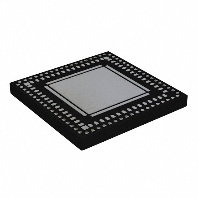
136-pin aQFN 10mm x 10mm package
Notes:
1. No purposely added lead. Fully EU Directive 2002/95/EC (RoHS), 2011/65/EU (RoHS 2) & 2015/863/EU (RoHS 3) compliant.
2. See https://www.diodes.com/quality/lead-free/ for more information about Diodes Incorporated’s definitions of Halogen- and Antimony-free, "Green" and Lead-free.
3. Halogen- and Antimony-free "Green” products are defined as those which contain