PI90LV044, PI90LVB044
LVDS Dual 2x2 Crosspoint/Repeater Switch
Features
Description
Dual 2x2 Crosspoint/Repeater Switch
Meets or Exceeds the Requirements of
ANSI TIA/EIA-644-1995
Designed for Signaling Rates up to 650 Mbit/s (325Mhz)
Operates from a single 3.3V Supply: –40°C to 85°C
Low-Voltage Differential Signaling with Output Voltages of
±350mV into:
- 100Ω load (PI90LV044)
- 50Ω load Bus LVDS Signaling (PI90LVB044)
Accepts ±350mV differential inputs
Wide common mode input range: 0.2V to 2.7V
Output drivers are high impedance when disabled or
when VCC 1.5V
Inputs are open, short, and terminated fail safe
Propagation Delay Time: 3.5ns
ESD protection is 10kV on bus pins
Bus Pins are High Impedance when disabled or
with VCC less than 1.5V
TTL Inputs are 5V Tolerant
Power Dissipation at 400 Mbit/s of 250mW
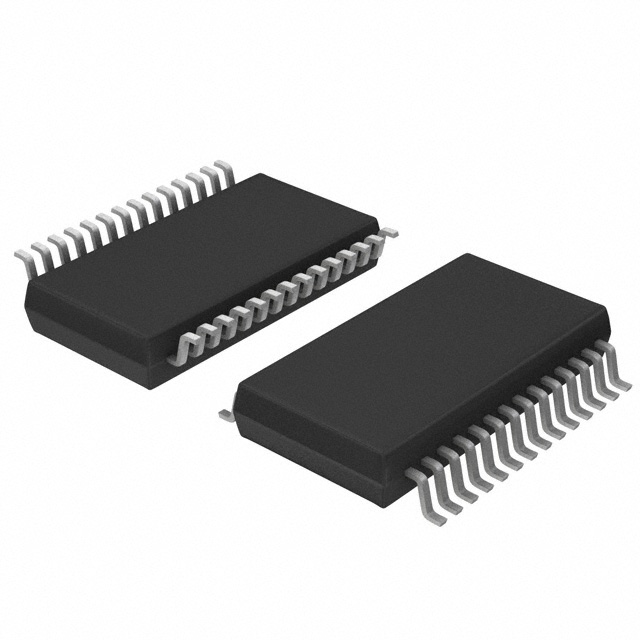
Packaging (Pb-free & Green available):
- 28-pin TSSOP (L)
The PI90LV044 and PI90LVB044 are monolithic dual 2x2 asynchronous crosspoint/repeater switches. The crosspoint function
is based on a multiplexer tree architecture. Each 2x2 switch can
be considered as a pair of 2:1 multiplexers that share the same
inputs. The signal path through each switch is fully differential
with minimal propagation delay. The signal path is unregistered,
so no clock is required for the data inputs. The signal line drivers
and receivers use Low Voltage Differential Signaling (LVDS) to
achieve signaling rates as high as 650Mbps.
The LVDS standard provides a minimum differential output voltage magnitude of 247 mV into a 100Ω load and receipt of 100
mV signals with up to 1V of ground potential difference between a
transmitter and receiver. The PI90LVB044 doubles the output drive
current to achieve LVDS levels with a 50 ohm load.
The intended application of these devices is for loop-through and
redundant channel switching for both point-to-point baseband
(PI90LV044) and multipoint (PI90LVB044) data transmissions
over controlled impedance media.
Pin Configuration
Block Diagram
S0,S1
1A/1B
2A/2B
3A/3B
4A/4B
S2/S3
09-0003
1DE/2DE
1Y/1Z
2Y/2Z
3Y/3Z
4Y/4Z
1B
1
28
VCC
1A
2
27
1Y
S0
3
26
1Z
1DE
4
25
2DE
S1
5
24
2Z
2A
6
23
2Y
2B
7
22
GND
3A
8
21
VCC
3B
9
20
3Y
S2
10
19
3Z
3DE
11
18
4DE
S3
12
17
4Y
4A
13
16
4Z
14
15
GND
4B
3DE/4DE
1
PS8485G
10/16/09
�PI90LV044, PI90LVB044
LVDS Dual 2x2 Crosspoint/Repeater Switch
MUX Truth Table
Input
Output
Function
S3, S1
S2, S0
1Y/1Z - 3Y/3Z
2T/2Z - 4Y/4Z
0
0
1A/1B - 3A/3B
1A/1B - 3A/3B
Splitter
0
1
2A/2B - 4A/4B
2A/2B - 4A/4B
Splitter
1
0
1A/1B - 3A/3B
1A/1B - 3A/3B
Router
1
1
2A/2B - 4A/4B
2A/2B - 4A/4B
Router
Note:
1. Setting nDE to 0 will set Ouput nY/nZ to High Impedance.
S1/S0
1DE/2DE
1A/1B
1Y/1Z
2A/2B
2Y/2Z
S3/S2
3DE/4DE
3A/3B
3Y/3Z
4A/4B
4Y/4Z
Cross Point
Router
Pass Through
Router
Router Options
S1/S0
1DE/2DE
1A/1B
1Y/1Z
2A/2B
2Y/2Z
S3/S2
3DE/4DE
3A/3B
3Y/3Z
4A/4B
4Y/4Z
Splitter A
Splitter B
Splitter Options
Figure 1. Possible Signal Routing
09-0003
2
PS8485G
10/16/09
�PI90LV044, PI90LVB044
LVDS Dual 2x2 Crosspoint/Repeater Switch
Absolute Maximum Ratings Over Operating Free-Air Temperature(1)
Supply Voltage Range, VCC(1)....................................................................... –0.5V to 4V
Voltage Range (DE, S0, S1) ...............................................................–0.5 to 6V
Input Voltage Range, VI (A or B) ..................................... –0.5V to VCC + 0.5V
Electrostatic Discharge: A, B, Y, Z, and GND(2)......... Class 3, A: 16kV, B:600V
All Pins..................................................... Class 3, A: 7kV, B:500V
Storage Temperature Range ......................................................–65°C to 150°C
Lead Temperature 1, 6 mm (1/16 inch) from case for 10 seconds ........... 260°C
Notes:
1. Stresses beyond those listed under "Absolute Maximum Ratings" may cause permanent damage to the device. These are stress ratings only, and
functional operation of the device at these or any other conditions beyond those indicated under "Recommended Operating Conditions" is not
implied. Exposure to Absolute-Maximum-Rated conditions for extended periods may affect device reliability.
2. All voltage values, except differential I/O bus voltages, are with respect to ground terminal.
3. Tested in accordance with MIL-STD-883C Method 3015.7
Recommended Operating Conditions
Supply Voltage, VCC
High-Level input voltage, VIH
S1 - S3, 1DE - 4DE
Min.
Nom.
Max.
Units
3.0
3.3
3.6
V
2
Low-Level input voltage, VIL
0.8
Magnitude of Differential Input Voltage | VID |
0.1
Common Mode input voltage, VIC (see figure 2)
| VID |
2
0.6
2.4 -
| VID |
2
VCC - 0.8
Operating free-air Temperature, TA
09-0003
-40
3
85
ºC
PS8485G
10/16/09
�PI90LV044, PI90LVB044
LVDS Dual 2x2 Crosspoint/Repeater Switch
2.5
VIC – Common-Mode Input Voltage – V
MAX at VCC > 3.15V
MAX at VCC = 3V
2
1.5
1
0.5
MIN
0
0.1
0.2
0.3
0.4
0.5
0.6
VID – Differential Input Voltage – V
Figure 2. Common-Mode Input Voltage vs. Differential Voltage
Receiver Electrical Characteristics Over Recommended Operating Conditions (unless otherwise noted)
Symbol
Parameter
VITH+
Positive going differential input voltage threshold
VITH-
Negative going differential input voltage threshold
II
Test Conditions
VCM = 1.2V
Input current (A or B inputs)
II (OFF)
Power-off input current (A or B inputs)
09-0003
Typ.(1)
Max.
100
-100
VI = 0V
-2
VI = 2.4V
-1.2
VCC = 0V
4
Min.
Units
mV
-20
μA
20
PS8485G
10/16/09
�PI90LV044, PI90LVB044
LVDS Dual 2x2 Crosspoint/Repeater Switch
Receiver/Driver Electrical Characteristics Over Recommended Operating Conditions (unless otherwise noted)
Symbol
Parameter
Test Condition
Min.
Typ.(1)
Max.
440
590
VOD
Differential Output voltage magnitude
247
∆VOD
Change in differential Output voltage magnitude
between logic states
-50
50
VOC(SS)
Steady-state common-mode output voltage
1.062
1.375
∆VOC(SS)
Change in steady-state common-mode output
voltage between logic states
VOC(PP)
Peak-to-peak common-mode output voltage
ICC
RL = 100Ω (LV)
RL = 50Ω (LVB)
-50
High level input current
IIL
Low level input current
IOS
Short circuit output current
IOZ
High impedence output current
IO(OFF)
Power off output current
CIN
Input Capacitance
50
mV
V
mV
150
No load
16
24
RL = 100Ω (LV)
26
40
RL = 50Ω (LVB)
42
54
All Channels Disabled
6
12
Supply Current
IIH
3
Units
DE
VIH = 5
S1, S2, S3, S4
DE
VIL = 0.8V
S1, S2, S3, S4
VOY or VOZ = 0V,
VOD = 0V
40
nA
-3
μA
-20
nA
10
μA
-10
mA
VOD = 600mV
1.5
±25
VO - 0V or VCC
1.5
±25
VCC = 0V, VO = 3.6V
1.5
±40
S0 - S3, 1DE - 4DE
mA
3
nA
pF
8
Note:
1. All typical values are at 25°C and with a 3.3 supply
09-0003
5
PS8485G
10/16/09
�PI90LV044, PI90LVB044
LVDS Dual 2x2 Crosspoint/Repeater Switch
Differential Receiver to Driver Switching Characteristics Over Recommended Operating Conditions
(unless otherwise noted)
Symbol
Parameter
Test Condition
Min.
Typ.(1)
Max.
tPLH
Differential propagation delay, low-to-high
4.0
6.0
tPHL
Differential propagation delay, high-to-low
4.0
6.0
tsk(p)
Pulse skew ( | tPHL = tPLH | )
0.25
0.3
tr
Transition, low-to-high
1.0
1.5
LVB044
0.8
1.3
tf
Transition, high-to-low
LV044
1.0
1.5
LVB044
0.8
1.3
tPHZ
Propagation delay time, high-level-to-high-impedence output
4.0
10
tPLZ
Propagation delay time, low-level-to-high-impedance output
4.3
10
tPZH
Propagation delay time, high-impedence to high-level output
3.0
10
tPZL
Propagation delay time, high-impdeence tolow-level output
2.0
10
-
95
-
95
-
95
-
95
LV044
CL = 10pF
tPHL_R1_Dx
tPLH_R1_Dx
tPHL_R2_Dx
Channel-tochannel skew, receiver to driver(2)
tPLH_R2_Dx
Units
ns
ps
Notes:
1. All typical values are at 25°C and with a 3.3 supply
2. These parametric values are measured over supply voltage and temperature ranges recommended for the device
09-0003
6
PS8485G
10/16/09
�PI90LV044, PI90LVB044
LVDS Dual 2x2 Crosspoint/Repeater Switch
Parameter Measurement Information
DE
Y
A
Pulse
Generator
R
B
D
Input
(see Note A)
VI(B)
1.4 V
VI(A)
1V
VOD
Z
RL (see Note B)
CL = 10 pF
(2 Places)
(see Note C)
100%
80%
VOD
0
20%
0%
tf
tr
Notes: A. All input pulses are supplied by a generator having the following characteristics: tr or tf ≤ 1ns, pulse repetition rate (PRR) - 50 Mpps,
pulse width = 10 ±0.2ns.
B. RL = 100Ω or 50Ω ±1%.
C. CL includes instrumentation and fixture capacitance within 6mm of the D.U.T.
D. The measurement of VOC(PP) is made on test equipment with a –3dB bandwidth of at least 300 MHz.
Figure 3. Test Circuit and Voltage Definitions for the Differential Output Signal
DE
Y
A
Pulse
Generator
R
RL (see Note B)
(2 Places)
D
B
Input
(see Note A)
Z
1.4 V
VI(A)
1V
VOC(PP)
(see Note D)
VOC
CL = 10 pF
(2 Places)
(see Note C)
VI(B)
VOC(SS)
VCC
Notes: A. All input pulses are supplied by a generator having the following characteristics: tr or tf ≤ 1ns, pulse repetition rate (PRR) - 50 Mpps,
pulse width = 10 ±0.2ns.
B. RL = 100Ω or 50Ω ±1%.
C. CL includes instrumentation and fixture capacitance within 6mm of the D.U.T.
D. The measurement of VOC(PP) is made on test equipment with a –3dB bandwidth of at least 300 MHz.
Figure 4. Test Circuit and Definitions for the Driver Common-Mode Output Voltage
09-0003
7
PS8485G
10/16/09
�PI90LV044, PI90LVB044
LVDS Dual 2x2 Crosspoint/Repeater Switch
DE
A
Pulse
Generator
Y
R
D
RL (see Note A)
Z
B
10 pF
10 pF
VIB
1.4 V
0-V Differential
1.2-V CM
1V
VIA
tPLH
tPHL
VOZ
1.4 V
0-V Differential
1.2-V CM
VOY
1V
80%
0-V Differential
20%
VOY – VOZ
tr
tf
Notes: A. RL = 100Ω or 50Ω ±1%
B. All input pulses are supplies by a generator having the following characteristics:
pulse repetition rate (PPR) = 50 Mpps, pulse width = 10 ±0.2ns.
Figure 5. Differential Receiver to Driver Propagation Delay and Driver Transition Time Waveforms
09-0003
8
PS8485G
10/16/09
�PI90LV044, PI90LVB044
LVDS Dual 2x2 Crosspoint/Repeater Switch
DE
1 V or 1.4 V
A
R
1.2 V
RL/2
(see Note A)
Y
1.2 V
D
B
Z
RL/2
(see Note A)
2V
DE
1.4 V
0.8 V
tPZH
tPHZ
≈ 1.4 V
VOY or VOZ
1.25 V
1.2 V
tPZL
tPLZ
1.2 V
1.15 V
VOY or VOZ
≈1 V
Notes:
A. RL = 100 Ω or 50 Ω ±1%
B. All input pulses are supplied by a generator having the following characteristics: pulse repetition rate (PRR) = 0.5 Mpps,
pulse width = 500 ±10ns.
Figure 6. Enable and Disable Timing Circuit
09-0003
9
PS8485G
10/16/09
�PI90LV044, PI90LVB044
LVDS Dual 2x2 Crosspoint/Repeater Switch
Typical Characteristics
PI90LV044
PI90LV044
HIGH-LEVEL OUTPUT VOLTAGE
vs
HIGH-LEVEL OUTPUT CURRENT
LOW-LEVEL OUTPUT VOLTAGE
vs
LOW-LEVEL OUTPUT CURRENT
4
VCC = 3.3 V
TA = 25°C
3
V OL – Low-Level Output Voltage – V
V OH – High-Level Ouptut Voltage – V
3.5
2.5
2
1.5
1
VCC = 3.3 V
TA = 25°C
3
2
1
.5
0
0
–4
–3
–2
0
0
–1
IOH – High-Level Output Current – mA
6
Figure 8
Figure 7
PI90LVB044
PI90LVB044
HIGH-LEVEL OUTPUT VOLTAGE
vs
HIGH-LEVEL OUTPUT CURRENT
LOW-LEVEL OUTPUT VOLTAGE
vs
LOW-LEVEL OUTPUT CURRENT
4
3.5
VCC = 3.3 V
TA = 25°C
3
V OL – Low-Level Output Voltage – V
V OH – High-Level Output Voltage – V
4
2
IOL – Low-Level Output Current – mA
2.5
2
1.5
1
.5
VCC = 3.3 V
TA = 25°C
3
2
1
0
0
–8
–6
–4
–2
0
0
IOH – High-Level Output Current – mA
4
6
8
10
12
Figure 10
Figure 9
09-0003
2
IOL – Low-Level Output Current – mA
10
PS8485G
10/16/09
�PI90LV044, PI90LVB044
LVDS Dual 2x2 Crosspoint/Repeater Switch
Packaging Mechanical: 28-Pin TSSOP (L)
DOCUMENT CONTROL NO.
PD - 1313
REVISION: D
28
DATE: 03/09/05
.169
.177
4.3
4.5
.004
.008
1
.378
.386
9.6
9.8
0.45
0.75
0.09
0.20
.018
.030
.252
BSC
6.4
.047
1.20
Max
SEATING
PLANE
.007
.012
0.19
0.30
.0256
BSC
0.65
.002
.006
0.05
0.15
Pericom Semiconductor Corporation
3545 N. 1st Street, San Jose, CA 95134
1-800-435-2335 • www.pericom.com
Note:
1. Package Outline Exclusive of Mold Flash and Metal Burr
2. Controlling dimentions in millimeters
3. Ref: JEDEC MO-153F/AE
DESCRIPTION: 28-Pin, 173-Mil Wide, TSSOP
PACKAGE CODE: L
Note:
• For latest package info, please check: http://www.pericom.com/products/packaging/mechanicals.php
Ordering Information
Ordering Code
Package Code
Package Type
PI90LV044LE
L
Pb-free & Green, 28-pin 170-mil TSSOP
PI90LVB044LE
L
Pb-free & Green, 28-pin 170-mil TSSOP
Notes:
• Thermal characteristics can be found on the company web site at www.pericom.com/packaging/
• E = Pb-free and Green
• Adding X suffix = Tape/Reel
Pericom Semiconductor Corporation • 1-800-435-2336 • www.pericom.com
09-0003
11
PS8485G
10/16/09
�