SM-8 DUAL N-CHANNEL ENHANCEMENT
MODE AVALANCHE RATED MOSFET
ZDM4206N
ISSUE 1 - NOVEMBER 1995
D1
G1
D1
S1
D2
G2
D2
S2
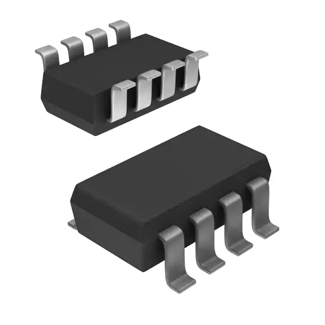
SM-8
(8 LEAD SOT223)
PARTMARKING DETAIL – M4206N
ABSOLUTE MAXIMUM RATINGS.
PARAMETER
SYMBOL
VALUE
UNIT
Drain-Source Voltage
VDS
60
V
Continuous Drain Current at Tamb=25°C
ID
1
A
Pulsed Drain Current
IDM
8
A
Gate-Source Voltage
VGS
± 20
V
Continuous Body Diode Current at Tamb =25°C
ISD
1
A
Avalanche Current – Repetitive
IAR
600
mA
Avalanche Energy – Repetitive
EAR
15
mJ
Operating and Storage Temperature Range
Tj:Tstg
-55 to +150
°C
THERMAL CHARACTERISTICS
PARAMETER
SYMBOL
Total Power Dissipation at Tamb = 25°C*
Any single die “on”
Both die “on” equally
Ptot
Derate above 25°C*
Any single die “on”
Both die “on” equally
Thermal Resistance - Junction to Ambient*
Any single die “on”
Both die “on” equally
VALUE
UNIT
2.25
2.75
W
W
18
22
mW/ °C
mW/ °C
55.6
45.5
°C/ W
°C/ W
* The power which can be dissipated assuming the device is mounted in a typical manner on a PCB
with copper equal to 2 inches square.
3 - 317
�ZDM4206N
ZDM4206N
TYPICAL CHARACTERISTICS
ELECTRICAL CHARACTERISTICS (at Tamb = 25°C unless otherwise stated).
Gate-Source Threshold Voltage
VGS(th)
Gate-Body Leakage
Zero Gate Voltage Drain Current
V
V
ID=1mA, VDS= VGS
IGSS
100
nA
VGS=± 20V, VDS=0V
IDSS
10
100
µA
µA
VDS=60V, VGS=0
VDS=48V, VGS=0V, T=125°C(2)
ID(on)
Static Drain-Source On-State
Resistance (1)
RDS(on)
1.3
ID=1mA, VGS=0V
3
On-State Drain Current(1)
Forward Transconductance(1)(2)
60
3
1
1.5
gfs
300
A
VDS=25V, VGS=10V
Ω
Ω
VGS=10V,ID=1.5A
VGS=5V,ID=0.5A
mS
Input Capacitance (2)
Ciss
100
pF
Common Source Output
Capacitance (2)
Coss
60
pF
Reverse Transfer Capacitance (2) Crss
20
pF
Turn-On Delay Time (2)(3)
td(on)
8
ns
Rise Time (2)(3)
tr
12
ns
Turn-Off Delay Time (2)(3)
td(off)
12
ns
Fall Time (2)(3)
tf
15
ns
10
8
6
4
ID=
3A
1.5A
0.5A
2
2
4
6
8
VDS=25V,ID=1.5A
VDD ≈25V, ID=1.5A,VGEN=10V
0
0
10
20
30
40
5V
4.5V
4V
3.5V
50
8
6
10V
9V
8V
4
2
0
2
4
6
8
VDS - Drain Source Voltage (Volts)
VDS - Drain Source Voltage (Volts)
Output Characteristics
Saturation Characteristics
4.5V
VGS=3.5V
10
6
8
10
8V 10V
6V
2.6
14V
1.0
20V
20V
0.1
0.1
2.4
VGS=10V
ID=1.5A
2.2
2.0
e
nc
ta
sis
e
eR
rc
ou
-S
n
ai
Dr
1.8
1.6
1.4
1.2
7V
6V
5V
4.5V
4V
3.5V
10
0.8
Gate Threshold Voltage VGS(TH)
0.6
-50 -25
900
800
VDS=10V
500
400
300
200
100
0
2
3
4
5
25 50 75 100 125 150 175 200 225
Normalised RDS(on) and VGS(th) v Temperature
1000
1
0
Tj-Junction Temperature (°C)
900
800
0
VGS=VDS
ID=1mA
1.0
1000
700
600
)
on
S(
RD
10
1.0
6
7
8
9
10
700
600
VDS=10V
500
400
300
200
100
0
0
1
2
3
4
5
6
7
8
9
10
VGS-Gate Source Voltage (Volts)
ID- Drain Current (Amps)
Transconductance v drain current
3 - 318
4
VGS-Gate Source Voltage (Volts)
gfs-Transconductance (mS)
6V
2
VGS=
20V
16V
14V
12V
gfs-Transconductance (mS)
7V
ID - Drain Current (Amps)
ID - Drain Current (Amps)
4
2
Transfer Characteristics
On-resistance v drain current
10V
9V
8V
0
10
ID-Drain Current (Amps)
10
6
2
VDS=25V, VGS=0V, f=1MHz
TYPICAL CHARACTERISTICS
8
4
Voltage Saturation Characteristics
(3) Switching times measured with 50Ω source impedance and
很抱歉,暂时无法提供与“ZDM4206NTC”相匹配的价格&库存,您可以联系我们找货
免费人工找货