2.85 VOLT ULTRA LOW DROPOUT
REGULATOR
ZLDO285
ISSUE 2 - JUNE 1997
DEVICE DESCRIPTION
FEATURES
The ZLDO Series low dropout linear regulators
operate with an exceptionally low dropout
voltage, typically only 30mV with a load
current of 100mA. The regulator series features
output voltages in the range 2.85 to 12 volts, this
device provides an output voltage of 2.85 volts.
•
•
•
•
•
•
•
•
•
•
•
The ZLDO285 consumes a typical quiescent
current of only 1mA at its maximum rated
output current of 300mA. A battery low flag is
available to indicate potential power fail
situations. If the input voltage falls to within
200mV of the regulated output voltage then the
error output pulls low. The device also features
an active high disable control. Once disabled
the ZLDO quiescent current falls to typically
11µA.
Very low dropout voltage
6mV dropout at 10mA output
30mV dropout at 100mA output
100mV dropout at 300mA output
2.85 volt fixed output
Other voltages available
Low quiescent current
1mA quiescent (typ) at 300mA output
Low battery flag
Shutdown control
Surface mount package
APPLICATIONS
•
•
•
•
•
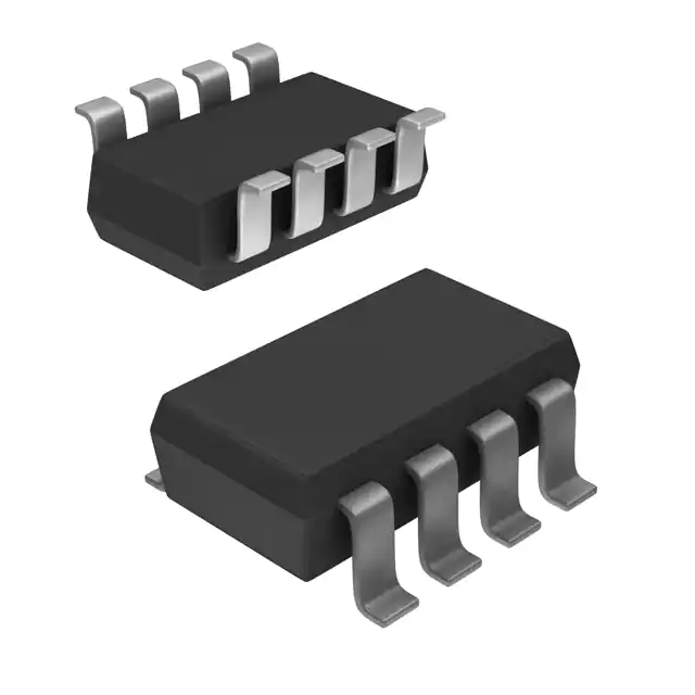
The ZLDO devices are packaged in Zetex SM8
8 pin small outline surface mount package,
ideal for applications where space saving is
important. The device low dropout voltage,
low quiescent current and small size make it
ideal for low power and battery powered
applications. Battery powered circuits can
make particular use of the low battery flag and
shutdown features.
Battery powered devices
Portable instruments
Portable communications
Laptop/Palmtop computers
Electronic organisers
Low Battery Flag
Vin
LOW BATTERY
COMPARATOR
THERMAL
SHUTDOWN
Vo
OUTPUT
DRIVE
BIAS
Shutdown
Control
CIRCUIT
Cs
SHUTDOWN
BANDGAP
REFERENCE
Shaping
Gnd
�ZLDO285
ABSOLUTE MAXIMUM RATING
Input Supply
Voltage Range
Shutdown Input
Voltage Range
Low Battery Output
Voltage Range
-0.3 to 20V
-0.3 to Vin
-0.3 to 20V
Output Current
Operating Temperature
Storage Temperature
Power Dissipation
(Tamb=25°C)
300mA
-40 to 85°C
-55 to 150°C
2W (Note 1)
ELECTRICAL CHARACTERISTICS
TEST CONDITIONS (Unless otherwise stated) Tamb =25°C,IL=10mA,Cs=10pF,Cout =1µF
Parameter
SYMBOL
CONDITIONS
MIN
TYP
MAX
UNITS
Output voltage
Vo
Vin=3.85V
2.75
2.85
2.95
V
Output voltage
temperature coefficient
Vo
∆T
Vin=3.85V
(Note 2, Note 4)
100
2 50
ppm/ °C
Line regulation
∆Vo
Vin=3.85to 20V
13
46
mV
Load regulation
∆Vo
IL=10 to 300mA
Vin=3.85V
38
66
mV
Dropout voltage
(Note3)
Vin-Vo
IL=10mA
IL=100mA
IL=300mA
6
30
100
10
75
200
mV
Quiescent current
Iq
Vin=3.85V, IL=0
0.55
1
mA
Quiescent current
at shutdown
Iqs
Vin=3.85V, IL=0,
Vshdn=Vin
11
30
µA
Shutdown control input Iins
current
Vshdn=Vin=3.85V
2
10
µA
Shutdown control
threshold voltage
Vin=3.85V
low(on)
high(off)
0.4
V
100
nA
Vts
1.5
Output current in
shutdown mode
(Note4)
ILs
Vin=20V
Vo=Gnd
50
Output noise voltage
(Note4)
en
Vin=3.85V
f=10Hz
to100kHz,
IL=100mA
140
Low battery detect
voltage
Vin(bld)
Low battery flag
output voltage
Vbl
Ibl=100µA,
VinVo+300mV
0.1
1
µA
Vo+0.2V
µV RMS
Vo+0.4V V
�ZLDO285
NOTES.
1. Maximum power dissipation of the device is calculated assuming the package is mounted on a PCB
measuring 2 inches square.
2 Output voltage temperature coefficient is calculated as:-
VO change x 1000000
VO x temperature change
3. Dropout voltage is defined as the input to output voltage differential at which the circuit ceases to
regulate. The value is measured when the output voltage has dropped by 100mV from V out measured
at the nominal input Vin = Vout + 1V
4. Guaranteed by design.
FUNCTIONAL DESCRIPTION
The ZLDO is a high performance, ultra low dropout, low quiescent regulator. Available in SM8 surface
mount packaging, the device is able to dissipate 2W(note 1) allowing complete design flexibility with
an input span upto 20V and 300mA output current. The device quiescent is 1mA (typ) at 300mA load
current. A low battery comparator signifies impending battery failure, whilst a shutdown function
reduces quiescent current to a mere 11µA (typ). A precision bandgap reference gives ± 2.5% output
tolerance and good temperature characteristics over the range -40 to +85°C. AC performance is
enhanced via the use of a small external capacitor.
PIN DEFINITIONS
Pin 1 LBF - Low Battery Flag. An open collector
NPN output which pulls low on failing input
supply.
Pin 2 SC - Shutdown Control. This high
impedance logic compatible input disables the
regulator when taken high. It includes a diode
wired to Vin and so will pass current if taken more
than 0.5V above Vin.
Pin 3 Vin - Voltage Input. The power supply to
the regulator. The permissible input voltage
range is -0.3 to 20V. An input capacitor is not
mandatory but will be useful in reducing the
coupling of noise from input to output and
minimising the effect of sudden changes in load
current on the input voltage.
Pin 4 N/C - Not Connected. Not internally
connected and so can be left open or wired to
any pin without affecting the performance of the
regulator.
Pin 5 Vout - Voltage Output. The output of the
regulator. An output capacitor of 1uF or greater
and having low ESR should be wired in close
proximity to the regulator to ensure stability for
all loads.
Pin 6 D/C - Do Not Connect. This pin is wired to
an internal circuit node of the regulator. No
external connection should be made to this pin.
Pin 7 Gnd - Ground. The ground connection of
the regulator against which the output voltage is
referenced.
Pin 8 Spg - Shaping. The shaping node for the
error amplifier of the regulator. A capacitor of
10pF wired from this pin to the output pin (pin 5)
gives optimum stability. Improved AC can be
achieved by reducing the value of this capacitor
but stability may be impaired for some load
conditions.
�ZLDO285
TYPICAL CHARACTERISTICS
1000
55
50
Ripple Rejection (dB)
Output Impedance (mΩ)
Cout = 1µF
800
600
10pF
4.7pF
2.2pF
400
200
0
100
10k
1k
100k
Cout=1uF
45
40
2.2pF
4.7pF
10pF
35
30
25
20
15
10
5
0
100
600
Vin=5v
Quiescent Current (uA)
Output Voltage (V)
Ripple Rejection v Frequency
Io=10mA
Vin=5v
2.900
2.850
2.800
2.750
-40
-20
0
20
40
60
560
520
480
440
400
-40
80
-20
Temperature (°C)
Vin=5v
16.0
14.0
12.0
10.0
8.0
0
20
40
20
40
60
80
Quiescent Current v Temperature
60
Temperature (°C)
Shutdown Current v Temperature
80
Vin=5v
Io=10mA
3.10
L.B.F. Operation Voltage (V)
Shutdown Current (µA)
18.0
-20
0
Temperature (°C)
Output Voltage Temperature Coefficient
6.0
-40
100K
Frequency (Hz)
Output Impedance v Frequency
2.950
10K
1K
Frequency (Hz)
3.09
3.08
3.07
3.06
3.05
3.04
-40
-20
0
20
40
60
80
Temperature (°C)
Low Battery Flag Operating Point
�ZLDO285
TYPICAL CHARACTERISTICS
220
Dropout Voltage (mV)
160
140
120
100
80
85°C
25°C
-40°C
60
40
20
0
0.1
10
1
100
1000
Load Current (mA)
Output Voltage Deviation (V)
Vin=10v
200
180
Vin=5v
0.8
0.4
-0.4
0
200
400
600
1000
Line Transient Response
1.0
Vin=5v
Io=100mA
10ms
1s
DC
Load Current (A)
Io=0mA
0.4
0
Output Voltage Deviation
-0.2
-0.4
0
800
Time (µs)
Dropout Voltage v Load Current
Output Voltage Deviation (V)
Io=100mA
Output Voltage Deviation
0
40
80
120
160
Time (µs)
Load Transient Response
200
0.1s
0.1
0.01
1
2
5
10
Input-Output Differential Voltage (V)
Safe Operating Area
Operation in shaded area is not guaranteed
20
�ZLDO285
APPLICATIONS
1). Simple 2.85V Supply
2). Post Converter Regulation
+5V In
+5V Out
IC1
ZLDO285
LBF Spg
SC
Gnd
Vin
D/C
C1
10pF
+2.85V Out
N/C Vout
C3
100nF
C2
1µF
0V In
0V Out
Figure 1
Using a circuit such as Figure 1, the ZLDO285 can
easily provide a 2.85V logic supply from an
available 5V rail where most standard regulators
could not guarantee correct operation. Although
this approach is not particularly energy efficient,
if the load taken at 2.85V is not too large, then the
added complexity and cost of a 2.85V switching
converter may not be justifiable and so this linear
solution can be preferable. This circuit will also
give far less noise than a switching regulator
which can be important when handling low level
analogue signals or low voltage measurements.
Voltage
Feedback
A common problem with multiple output switch
mode converters is that only one output can be
used in the feedback control loop of the switching
regulator. Thus only one output is fully regulated.
All other outputs are prone to tracking errors that
occur if the load on any output changes
significantly. By ensuring close coupling of all
transformer windings and minimising the
impedance of all outputs, these errors can be
reduced but never eliminated. A simple way
round this problem is to wind the switching
regulator transformer to give a slightly higher
voltage than required and regulate down from
this to the desired voltage with a linear regulator.
This is indicated in Figure 2. To keep losses low
and so maintain the advantages of a switch
mode supply, it is important that the voltage drop
across this regulator is kept as low as possible,
i.e. just high enough to compensate for the poor
output impedance of the switching power supply
but no higher. The low dropout voltage of the
ZLDO285 allows this circuit technique to be
implemented very effectively, giving a highly
stable and accurate low noise supply.
D1
+5V Out
TR1
Switching
Regulator
C4
220µF
D2
ZLDO285
LBF Spg
SC Gnd
Vin D/C
C1
10pF
+2.85V Out
N/C Vout
C5
Figure 2
C2
1µF
220µF
0V Out
�ZLDO285
APPLICATIONS
3). Low Battery Flag
4). Over Temperature Shutdown
The ZLDO285 provides an output called Low
Battery Flag (LBF). Unlike many regulators that
only signal that they are falling out of regulation,
the LBF output of the ZLDO285 indicates that the
voltage drop across the regulator has fallen to
less than typically 300mV and so supply failure is
imminent.
The ZLDO285 regulator includes an over
temperature shutdown circuit that disables the
regulator if its chip temperature should exceed
125°C for any reason. Although intended to
provide a limited guard against excessive internal
power dissipation, this circuit will shut down the
regulator if its ambient rises above 125°C.
ZLDO285
LBF Spg
SC Gnd
Vin D/C
C1
10pF
+2.85V
N/C Vout
4.8V
C3
100nF
C2
1µF
R1
100k
Microproc.
System
Interrupt
Input
0V
Figure 3
This improved warning gives both more time for
the system supplied to shutdown gracefully and
maintains regulation while this happens. This
could be a vital point if measurements are under
way and must be completed accurately for
instance. The LBF output is driven by an open
collector NPN transistor which pulls low when
the supply to the regulator is failing. Figure 3
shows this output being used. Note that resistor
R1 is necessary only if the interrupt logic does not
include a pull-up resistor.
Thus, the regulator could be used to disable a
circuit in the event of the ambient temperature
within which the circuit is mounted becoming
too high. Any internal power dissipation caused
as a result of supplying load current, will reduce
the ambient temperature at which shutdown
occurs. Note that to achieve the extremely low
dropout voltage and high current performance
provided by the ZLDO devices, the parts can be
damaged by sustained output shorts or
excessive loads when combined with high input
supply voltages. To ensure reliable operation,
keep loads within the SOA graph boundaries
indicated in the typical characteristics.
�ZLDO285
APPLICATIONS
5). Logic Controlled Power Supply
Fig.4 shows all that is necessary to allow a
microprocessor to control a power supply based
on the ZLDO285. The Shutdown Control pin (pin
2), is a logic compatible input that disables the
regulator when a voltage in excess of 1.5V is
applied. The current required to drive this input
is less than 10µA. When the regulator is
shutdown in this way, the quiescent current of
the ZLDO285 falls to around 11µA. This makes
the regulator suitable for a wide range of battery
powered applications where intermittent
operation occurs. The shutdown control pin
should not be taken to a voltage higher than Vin
if low quiescent supply current is important. The
shutdown control is a high impedance input and
so if not required, should be wired to the ground
pin (pin 7).
+5.0V
to 20V
IC2
ZLDO285
Vin Vout
Gnd
IC1
ZSR330
LBF Spg
Microproc.
System
SC Gnd
Vin D/C
Supply Input
N/C Vout
C3
100nF
0V
Figure 4
C1
10pF
+2.85V
C2
1µF
Switched
Output
0V
�ZLDO285
Connection Diagram
SM8 Package Suffix – T8
Top View –
Pin 6 must be left floating
Ordering Information
Part Number
Package
Part Mark
ZLDO285T8
SM8
ZLDO285
�
很抱歉,暂时无法提供与“ZLDO285T8TA”相匹配的价格&库存,您可以联系我们找货
免费人工找货