2.85 TO 12 VOLT FIXED POSITIVE
LOCAL VOLTAGE REGULATOR
ZR78L
SERIES
ISSUE 3 - DECEMBER 2001
DEVICE DESCRIPTION
FEATURES
The ZR78L Series three terminal fixed positive
voltage regulators feature internal circuit
current limit and thermal shutdown making
the devices difficult to destroy. The circuit
design allows creation of any custom voltage
in the range 2.85 to 12 volts. The devices are
available in a small outline surface mount
package, ideal for applications where space
saving is important, as well as through hole
TO92 style packaging. The devices are suited
to local voltage regulation applications, where
problems could be encountered with
distributed single source regulation, as well as
more general voltage regulation applications.
•
•
•
•
•
•
•
•
•
•
•
The ZR78L Series show performance
characteristics superior to other local voltage
regulators. The initial output voltage is
maintained to within 2.5% with a quiescent
current of typically 350µA. Output voltage
change, with input voltage and load current, is
much lower than competitive devices. The
ZR78L devices are completely stable with no
external components. The device will shut
down under thermal overload conditions but
as the device cools, regulation will restart.
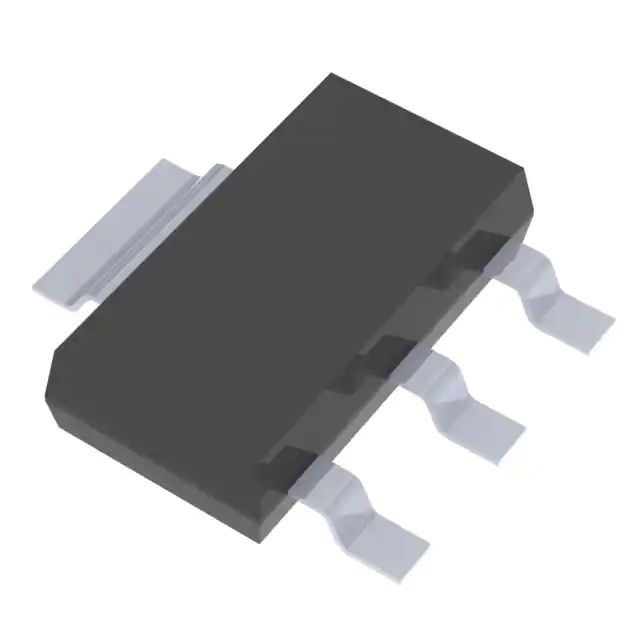
Small outline SOT223 package
SO8 package (3.3V and 5.0V)
TO92 package
2.85 to 12 Volt
Output current up to 200mA
Tight initial tolerance
Low quiescent current
-55 to 125°C temperature range
No external components
Internal thermal shutdown
Internal short circuit current limit
VOLTAGE RANGE
4-200
ZR78L028
2.85V
ZR78L03
3.0V
ZR78L033
3.3V
ZR78L04
4.0V
ZR78L048
4.85V
ZR78L05
5.0V
ZR78L052
5.2V
ZR78L057
5.7V
ZR78L06
6.0V
ZR78L07
7.0V
ZR78L08
8.0V
ZR78L085
8.5V
ZR78L09
9.0V
ZR78L10
10.0V
ZR78L12
12.0V
�ZR78L
SERIES
ABSOLUTE MAXIMUM RATING
Input voltage
20V
Output Current(Io) 200mA
Operating Temperature -55 to 125°C
Storage Temperature
-65 to 150°C
Power Dissipation (Tamb=25°C)
SOT223
2W(Note 3)
TO92
600mW
S08
780mW(Note 3)
ELECTRICAL CHARACTERISTICS:
Notes:
1. The maximum operating input voltage and
output current of the device will be governed by
the maximum power dissipation of the selected
package. Maximum package power dissipation is
specified at 25 °C and must be linearly derated to
zero at Tamb=125°C.
2. The following data represents pulse test
conditions with junction temperatures as
indicated at the initiation of the test. Continuous
operation of the devices with the stated conditions
might exceed the power dissipation limits of the
chosen package.
3. Maximum power dissipation, for the SOT223
and SO8 packages, is calculated assuming that the
device is mounted on a PCB measuring 2 inches
square.
4. The shut down feature of the device operates if
its temperature exceeds its design limit as might
occur during external faults, short circuits etc. If the
regulator is supplied from an inductive source
then a large voltage transient, on the regulator
input, can result should the shut down circuit
operate. It is advised that a capacitor (1µF or
greater) should be applied across the regulator
input to ensure that the maximum voltage rating
of the device is not exceeded under shutdown
conditions.
ZR78L028 TEST CONDITIONS (Unless otherwise stated):Tj=25°C, IO=100mA, Vin=6.85V
SYMBOL PARAMETER
VO
CONDITIONS
MIN.
TYP.
MAX.
UNITS
2.78
2.85
2.92
V
IO=1 to 200mA τ 2.736
2.964
V
Vin=4.85 to 20V
2.736
IO=1 to 100mA τ
2.964
V
Output Voltage
∆VO
Line Regulation
Vin=4.85 to 20V
10
40
mV
∆VO
Load Regulation
IO=1 to 200mA
IO=1 to 100mA
5
2
25
mV
mV
Quiescent Current
τ
350
600
µA
100
100
µA
µA
lq
∆lq
Quiescent Current Change IO=1 to 200mA
Vin=4.85 to 20V
Vn
Output Noise Voltage
∆Vin /∆VO Ripple Rejection
Vin
∆VO /∆T
Vin=5.85 to 18V
f=120Hz
Input Voltage Required To
Maintain Regulation
Average Temperature
Coefficient of VO
τ=Tj=-55 to 125°C
75
µV rms
48
62
dB
4.85
4.55
V
0.1
mV/°C
f=10Hz to 10kHz
IO=5.0mA τ
�ZR78L
SERIES
ZR78L03 TEST CONDITIONS (Unless otherwise stated):Tj=25°C, IO=100mA, Vin=7V
SYMBOL PARAMETER
VO
CONDITIONS
Output Voltage
MIN.
TYP.
2.92
3.0
MAX.
UNITS
3.08
V
IO=1 to 200mA τ 2.88
3.12
V
Vin=5 to 20V
2.88
IO=1 to 100mA τ
3.12
V
∆VO
Line Regulation
Vin=5 to 20V
10
40
mV
∆VO
Load Regulation
IO=1 to 200mA
IO=1 to 100mA
5
2
25
mV
mV
Quiescent Current
τ
350
600
µA
100
100
µA
µA
lq
∆lq
Quiescent Current Change IO=1 to 200mA
Vin=5 to 20V
Vn
Output Noise Voltage
∆Vin /∆VO Ripple Rejection
Vin
∆VO /∆T
Vin=6 to 18V
f=120Hz
Input Voltage Required To
Maintain Regulation
Average Temperature
Coefficient of VO
75
µV rms
48
62
dB
5
4.7
V
0.1
mV/°C
f=10Hz to 10kHz
IO=5.0mA τ
ZR78L033 TEST CONDITIONS (Unless otherwise stated):Tj=25°C, IO=100mA, Vin=7.3V
SYMBOL PARAMETER
VO
CONDITIONS
MIN.
TYP.
3.218
3.3
3.382
V
IO=1 to 200mA τ
3.168
3.432
V
Vin=5.3 to 20V
IO=1 to 100mA τ
3.168
3.432
V
Output Voltage
MAX.
UNITS
∆VO
Line Regulation
Vin=5.3 to 20V
7.5
30
mV
∆VO
Load Regulation
IO=1 to 200mA
IO=1 to 100mA
5
2
25
mV
mV
Quiescent Current
τ
350
600
µA
100
100
µA
µA
lq
∆lq
Quiescent Current Change IO=1 to 200mA
Vin=5.3 to 20V
Vn
Output Noise Voltage
∆Vin /∆VO Ripple Rejection
Vin
∆VO /∆T
Input Voltage Required To
Maintain Regulation
Average Temperature
Coefficient of VO
τ =Tj = -55 to 125 °C
50
µV rms
50
64
dB
5.3
5
V
0.1
mV/°C
f=10Hz to 10kHz
Vin=6.3 to 18V
f=120Hz
IO=5.0mA τ
�ZR78L
SERIES
ZR78L04 TEST CONDITIONS (Unless otherwise stated):Tj=25°C, IO=100mA, Vin=8V
SYMBOL PARAMETER
VO
CONDITIONS
Output Voltage
MIN.
TYP.
3.9
4.0
MAX.
UNITS
4.1
V
IO=1 to 200mA τ 3.84
4.16
V
Vin=6 to 20V
3.84
IO=1 to 100mA τ
4.16
V
∆VO
Line Regulation
Vin=6 to 20V
10
40
mV
∆VO
Load Regulation
IO=1 to 200mA
IO=1 to 100mA
5
2
25
mV
mV
Quiescent Current
τ
350
600
µA
100
100
µA
µA
lq
∆lq
Quiescent Current Change IO=1 to 200mA
Vin=6 to 20V
Vn
Output Noise Voltage
∆Vin /∆VO Ripple Rejection
Vin
∆VO /∆T
Vin=7 to 18V
f=120Hz
Input Voltage Required To
Maintain Regulation
Average Temperature
Coefficient of VO
75
µV rms
48
62
dB
6
5.3
V
0.1
mV/°C
f=10Hz to 10kHz
IO=5.0mA τ
ZR78L048 TEST CONDITIONS (Unless otherwise stated):Tj=25°C, IO=100mA, Vin=8.85V
SYMBOL PARAMETER
VO
CONDITIONS
Output Voltage
MIN.
TYP.
4.729
4.85
MAX.
UNITS
4.971
V
IO=1 to 200mA τ 4.656
5.044
V
Vin=6.8 to 20V
4.656
IO=1 to 100mA τ
5.044
V
∆VO
Line Regulation
Vin=6.85 to 20V
10
40
mV
∆VO
Load Regulation
IO=1 to 200mA
IO=1 to 100mA
5
2
25
mV
mV
Quiescent Current
τ
350
600
µA
100
100
µA
µA
lq
∆lq
Quiescent Current Change IO=1 to 200mA
Vin=6.85 to 20V
Vn
Output Noise Voltage
∆Vin /∆VO Ripple Rejection
Vin
∆VO /∆T
Vin=7.85 to 18V
f=120Hz
Input Voltage Required To
Maintain Regulation
Average Temperature
Coefficient of VO
τ =Tj = -55 to 125°C
50
µV rms
50
64
dB
6.85
6.55
V
0.1
mV/°C
f=10Hz to 10kHz
IO=5.0mA τ
�ZR78L
SERIES
ZR78L10TEST CONDITIONS (Unless otherwise stated):Tj=25°C, IO=100mA, Vin=14V
SYMBOL PARAMETER
VO
CONDITIONS
Output Voltage
MIN.
TYP.
MAX.
UNITS
9.75
10
10.25
V
IO=1 to 200mA τ
9.6
10.4
V
Vin=12 to 20V
IO=1 to 100mA τ
9.6
10.4
V
∆VO
Line Regulation
Vin=12 to 20V
12
40
mV
∆VO
Load Regulation
IO=1 to 200mA
IO=1 to 100mA
9
3
30
mV
mV
Quiescent Current
τ
350
600
µA
100
100
µA
µA
lq
∆lq
Quiescent Current Change IO=1 to 200mA
Vin=12 to 20V
Vn
Output Noise Voltage
∆Vin /∆VO Ripple Rejection
Vin
∆VO /∆T
f=10Hz to 10kHz
Vin=13 to 18V
f=120Hz
Input Voltage Required To
Maintain Regulation
Average Temperature
Coefficient of VO
43
12
IO=5.0mA τ
150
µV rms
57
dB
11.7
V
0.25
mV/°C
ZR78L12TEST CONDITIONS (Unless otherwise stated):Tj=25°C, IO=100mA, Vin=16V
SYMBOL PARAMETER
VO
CONDITIONS
Output Voltage
MIN.
TYP.
MAX.
UNITS
11.7
12
12.3
V
IO=1 to 200mA τ
11.52
12.48
V
Vin=14 to 20V
IO=1 to 100mA τ
11.52
12.48
V
∆VO
Line Regulation
Vin=14 to 20V
12
40
mV
∆VO
Load Regulation
IO=1 to 200mA
IO=1 to 100mA
9
3
30
mV
mV
Quiescent Current
τ
350
600
µA
100
100
µA
µA
lq
∆lq
Quiescent Current Change IO=1 to 200mA
Vin=14 to 20V
Vn
Output Noise Voltage
∆Vin /∆VO Ripple Rejection
Vin
∆VO /∆T
f=10Hz to 10kHz
Vin=15 to 18V
f=120Hz
Input Voltage Required To
Maintain Regulation
Average Temperature
Coefficient of VO
τ =Tj = -55 to 125 °C
43
14
IO=5.0mA τ
150
µV rms
57
dB
13.7
V
0.25
mV/°C
�ZR78L028 ZR78L03
ZR78L04 ZR78L057
ZR78L09
ZR78L
SERIES
TYPICAL CHARACTERISTICS
5.72
ZR78L03
3.00
5.70
2.99
5.68
2.98
Io= 5mA
Vin= Vo+ 4V
2.86
2.85
Output Voltage (V)
Output Voltage (V)
3.01
2.84
2.82
ZR78L057
5.66
Io= 5mA
Vin= Vo+ 4V
4.00
3.98
3.96
ZR78L04
ZR78L028
3.94
-50
-25
0
25
50
75
100 125
-50
-25
Temperature ( °C)
Output Voltage Temperature Coefficient
50
100 125
75
450
ZR78L09
Io= 0
Vin=Vo+ 4V
9.04
9.00
8.96
Quiescent Current (uA)
Io= 5mA
Vin= Vo+ 4V
Output Voltage (V)
25
Output Voltage Temperature Coefficient
9.08
8.92
400
350
300
250
-50
-25
0
25
50
75
100 125
-50
-25
Temperature ( C)
25
50
100 125
75
0
Output Voltage Temperature Coefficient
Quiescent Current vs. Temperature
2.5
400
2.0
Drop-Out Voltage (V)
500
300
200
Vo=0
Vin=10V
100
0
Temperature ( C)
0
Short-Circuit Output Current (mA)
0
Temperature ( °C)
0
Io=200mA
1.5
Io=100mA
1.0
0.5
0
-50
-25
0
25
50
75
100 125
Temperature ( C)
0
Peak Output Current vs. Temperature
-50
-25
0
25
50
75
100 125
Temperature ( C)
0
Drop-Out Voltage vs. Temperature
�ZR78L033 ZR78L05
ZR78L06
ZR78L08
ZR78L10
ZR78L
SERIES
TYPICAL CHARACTERISTICS
5.01
8.02
ZR78L05
8.00
4.99
4.98
IO = 5mA
V in = V O + 4V
3.30
3.29
Output Voltage (V)
Output Voltage (V)
5.00
7.98
ZR78L08
7.96
IO = 5mA
V in = V O + 4V
6.00
5.98
5.96
3.28
ZR78L06
ZR78L033
3.27
5.94
-50
-25
0
25
50
75
100
125
-50
-25
Temperature (° C)
IO = 5mA
V in = V O + 4V
10.04
10.00
9.96
Quiescent Current (uA)
ZR78L10
Output Voltage (V)
50
75
100
125
450
10.08
IO = 0
V in = V O + 4V
400
350
300
250
9.92
-50
-25
0
25
50
75
100
125
-50
-25
Temperature (° C)
0
25
50
75
100
125
Temperature (° C)
Output Voltage Temperature Coefficient
Quiescent Current v Temperature
500
2.5
400
2.0
Drop-Out Voltage (V)
Short-Circuit Output Current (mA)
25
Output Voltage Temperature Coefficient
Output Voltage Temperature Coefficient
300
200
100
0
Temperature (° C)
IO = 0
V in = 10V
IO= 200mA
1.5
IO= 100mA
1.0
0.5
0
0
-50
-25
0
25
50
75
100
125
-50
-25
0
25
50
75
100
125
Temperature (° C)
Temperature (° C)
Peak Output Current v Temperature
Drop-Out Voltage v Temperature
�ZR78L
SERIES
ZR78L057 TEST CONDITIONS (Unless otherwise stated):Tj=25°C, IO=100mA, Vin=9.7V
SYMBOL PARAMETER
VO
CONDITIONS
Output Voltage
MIN.
Typ.
5.557
5.7
MAX.
UNITS
5.843
V
IO=1 to 200mA τ 5.47
5.93
V
Vin=7.7 to 20V
IO=1 to 100mA τ
5.93
V
5.47
∆VO
Line Regulation
Vin=7.7 to 20V
10
40
mV
∆VO
Load Regulation
IO=1 to 200mA
IO=1 to 100mA
7
2.5
30
mV
mV
350
600
µA
100
100
µA
µA
Quiescent Current
τ
∆lq
Quiescent Current Change
IO=1 to 200mA
Vin=7.7 to 20V
Vn
Output Noise Voltage
f=10Hz to 10kHz
lq
∆Vin /∆VO Ripple Rejection
Vin
∆VO /∆T
Vin=8.7 to 18V
f=120Hz
Input Voltage Required To
Maintain Regulation
Average Temperature
Coefficient of VO
90
µV rms
48
62
dB
7.7
7.4
V
IO=5.0mA τ
0.15
mV/°C
ZR78L06 TEST CONDITIONS (Unless otherwise stated):Tj=25°C, IO=100mA, Vin=10V
SYMBOL PARAMETER
VO
CONDITIONS
Output Voltage
MIN.
TYP.
MAX.
UNITS
5.85
6
6.15
V
IO=1 to 200mA τ
5.76
6.24
V
Vin=8 to 20V
IO=1 to 100mA τ
5.76
6.24
V
∆VO
Line Regulation
Vin=8 to 20V
10
40
mV
∆VO
Load Regulation
IO=1 to 200mA
IO=1 to 100mA
7
2.5
30
mV
mV
350
600
µA
100
100
µA
µA
Quiescent Current
τ
∆lq
Quiescent Current Change
IO=1 to 200mA
Vin=8 to 20V
Vn
Output Noise Voltage
lq
∆Vin /∆VO Ripple Rejection
Vin
∆VO /∆T
Input Voltage Required To
Maintain Regulation
Average Temperature
Coefficient of VO
τ =Tj = -55 to 125 °C
90
µV rms
48
62
dB
8
7.7
V
0.15
mV/°C
f=10Hz to 10kHz
Vin=9 to 18V
f=120Hz
IO=5.0mA τ
�ZR78L
SERIES
ZR78L05 TEST CONDITIONS (Unless otherwise stated):Tj=25°C, IO=100mA, Vin=9V
SYMBOL PARAMETER
VO
CONDITIONS
MIN.
TYP.
4.875
5
5.125
V
IO=1 to 200mA τ
4.8
5.2
V
Vin=7 to 20V
IO=1 to 100mA τ
4.8
5.2
V
Output Voltage
MAX.
UNITS
∆VO
Line Regulation
Vin=7 to 20V
10
40
mV
∆VO
Load Regulation
IO=1 to 200mA
IO=1 to 100mA
5
2
25
mV
mV
Quiescent Current
τ
350
600
µA
100
100
µA
µA
lq
∆lq
Quiescent Current Change IO=1 to 200mA
Vin=7 to 20V
Vn
Output Noise Voltage
∆Vin /∆VO Ripple Rejection
Vin
∆VO /∆T
Vin=8 to 18V
f=120Hz
Input Voltage Required To
Maintain Regulation
Average Temperature
Coefficient of VO
75
µV rms
48
62
dB
7
6.7
V
0.1
mV/°C
f=10Hz to 10kHz
IO=5.0mA τ
ZR78L052 TEST CONDITIONS (Unless otherwise stated):Tj=25°C, IO=100mA, Vin=9.2V
SYMBOL PARAMETER
VO
CONDITIONS
Output Voltage
MIN.
TYP.
MAX.
UNITS
5.070
5.2
5.330
V
IO=1 to 200mA τ
4.99
5.41
V
Vin=7.2 to 20V
IO=1 to 100mA τ
4.99
5.41
V
∆VO
Line Regulation
Vin=7.2 to 20V
10
40
mV
∆VO
Load Regulation
IO=1 to 200mA
IO=1 to 100mA
5
2
25
mV
mV
Quiescent Current
τ
350
600
µA
100
100
µA
µA
lq
∆lq
Quiescent Current Change IO=1 to 200mA
Vin=7.2 to 20V
Vn
Output Noise Voltage
∆Vin /∆VO Ripple Rejection
Vin
∆VO /∆T
Input Voltage Required To
Maintain Regulation
Average Temperature
Coefficient of VO
τ =Tj = -55 to 125 °C
75
µV rms
48
62
dB
7.2
6.9
V
0.1
mV/°C
f=10Hz to 10kHz
Vin=8.2 to 18V
f=120Hz
IO=5.0mA τ
�ZR78L
SERIES
ZR78L085 TEST CONDITIONS (Unless otherwise stated):Tj=25°C, IO=100mA, Vin=12.5V
SYMBOL PARAMETER
VO
CONDITIONS
Output Voltage
MIN.
TYP.
MAX.
UNITS
8.288
8.5
8.712
V
IO=1 to 200mA τ
8.16
8.84
V
Vin=10 to 20V
IO=1 to 100mA τ
8.16
8.84
V
∆VO
Line Regulation
Vin=10.5 to 20V
11
40
mV
∆VO
Load Regulation
IO=1 to 200mA
IO=1 to 100mA
8
3
30
mV
mV
Quiescent Current
τ
350
600
µA
100
100
µA
µA
lq
∆lq
Quiescent Current Change IO=1 to 200mA
Vin=10.5 to 20V
Vn
Output Noise Voltage
∆Vin /∆VO Ripple Rejection
Vin
∆VO /∆T
f=10Hz to 10kHz
Vin=11.5 to 18V
f=120Hz
Input Voltage Required To
Maintain Regulation
Average Temperature
Coefficient of VO
44
10.5
IO=5.0mA τ
115
µV rms
60
dB
10.2
V
0.25
mV/°C
ZR78L09TEST CONDITIONS (Unless otherwise stated):Tj=25°C, IO=100mA, Vin=13V
SYMBOL PARAMETER
VO
CONDITIONS
Output Voltage
MIN.
TYP.
8.775
9.0
MAX.
UNITS
9.225
V
IO=1 to 200mA τ 8.64
9.36
V
Vin=11 to 20V
8.64
IO=1 to 100mA τ
9.36
V
∆VO
Line Regulation
Vin=11 to 20V
12
40
mV
∆VO
Load Regulation
IO=1 to 200mA
IO=1 to 100mA
9
3
30
mV
mV
Quiescent Current
τ
350
600
µA
100
100
µA
µA
lq
∆lq
Quiescent Current Change IO=1 to 200mA
Vin=11 to 20V
Vn
Output Noise Voltage
∆Vin /∆VO Ripple Rejection
Vin
∆VO /∆T
Vin=12 to 18V
f=120Hz
Input Voltage Required To
Maintain Regulation
Average Temperature
Coefficient of VO
τ =Tj = -55 to 125°C
150
µV rms
43
57
dB
11
10.7
V
f=10Hz to 10kHz
IO=5.0mA τ
0.25
mV/°C
�ZR78L
SERIES
ZR78L028 ZR78L03
ZR78L04 ZR78L057
ZR78L09
TYPICAL CHARACTERISTICS
90
Io = 100mA
VIN = VOUT+ 4V
1.0
ZR78L09
ZR78L057
ZR78L04
ZR78L03
ZR78L028
0.1
Io = 100mA
Vin = Vout + 3V
DVin = 200mV p/p
80
Ripple Rejection (dB)
Output Impedance (Ohms)
10
70
60
50
ZR78L028
ZR78L03
ZR78L04
40
ZR78L057
30
ZR78L09
20
10
0
10
0.01
100
1K
100K
10K
(VO + 9)
100 mA
(V + 4)
0
O
+0.5
OUTPUT VOLTAGE
DEVIATION
0
IO = 100mA
COUT = 0
dVIN /dt = 5V/µs
-1.0
0
10
20
30
40
50
Time (us)
Line Transient Response
Thermal Resistance (°C/W)
D=1
160
140
TO92 PACKAGE
120
100
D=0.5
80
60
D=0.2
40
D=0.1
20
0
1m
100K
+0.5
OUTPUT VOLTAGE
DEVIATION
0
-0.5
V IN = Vo+ 4V
COUT= 0
dIo /dt = 1A/µs
-1.0
0
10
20
30
40
50
Time (us)
Load Transient Response
48
40
D=1
SOT223 PACKAGE
32
D=0.5
24
16
D=0.2
D=0.1
8
D=0.05
D=0.05
D=0
D=0
0
10K
LOAD CURRENT
INPUT VOLTAGE
-0.5
1K
Ripple Rejection vs. Ripple Frequency
Output Voltage Deviation (V)
Output Voltage Deviation (V)
Output Impedance vs. Frequency
Thermal Resistance (°C/W)
100
Ripple Frequency (Hz)
Frequency (Hz)
0
10m 100m
1
10
Pulse Width (s)
Thermal Resistance v Pulse Width
1m
10m 100m
1
10
Pulse Width(s)
Thermal Resistance v Pulse Width
�ZR78L
SERIES
ZR78L033 ZR78L05
ZR78L06
ZR78L08
ZR78L10
TYPICAL CHARACTERISTICS
90
IO =100mA
VIN =VOUT+4V
1.0
ZR78L10
ZR78L08
ZR78L06
ZR78L05
ZR78L033
0.1
Io = 100mA
Vin = Vout + 3V
∆Vin = 200mV p/p
80
Ripple Rejection (dB)
Output Impedance (Ohms)
10
70
60
50
ZR78L033
ZR78L05
40
ZR78L06
ZR78L08
30
ZR78L10
20
10
0
10
0.01
1K
100K
10K
100
1K
Output Impedance v Frequency
Ripple Rejection v Ripple Frequency
(Vo + 9)
(Vo+ 4)
+0.5
OUTPUT VOLTAGE
DEVIATION
0
-0.5
Io=100mA
COUT=0
dVIN/dt =5V/us
-1.0
0
LOAD CURRENT
100 mA
0
+0.5
OUTPUT VOLTAGE
DEVIATION
0
-0.5
V IN= V O+ 4V
COUT= 0
dIO /dt =1A/µs
-1.0
10
30
20
40
50
0
10
48
Thermal Resistance ( C/W)
Thermal Resistance ( C/W)
50
Load Transient Response
D=1
140
TO92 PACKAGE
120
100
D=0.5
80
60
0
40
Time (µs)
Line Transient Response
20
30
20
Time (µs)
40
100K
Ripple Frequency (Hz)
INPUT VOLTAGE
160
10K
Frequency (Hz)
Output Voltage Deviation (V)
Output Voltage Deviation (V)
100
D=0.2
D=0.1
40
SOT223 PACKAGE
32
24
16
8
D=0.05
D=0
1ms
10
100
1s
10
Pulse Width
Thermal Resistance v Pulse Width
0
1ms
10
100
1s
10
Pulse Width
Thermal Resistance v Pulse Width
�ZR78L
SERIES
ZR78L07 TEST CONDITIONS (Unless otherwise stated):Tj=25°C, IO=100mA, Vin=11V
SYMBOL PARAMETER
VO
CONDITIONS
Output Voltage
MIN.
TYP.
MAX.
UNITS
6.825
7
7.175
V
IO=1 to 200mA τ
6.72
7.28
V
Vin=9 to 20V
IO=1 to 100mA τ
6.72
7.28
V
∆VO
Line Regulation
Vin=9 to 20V
10
40
mV
∆VO
Load Regulation
IO=1 to 200mA
IO=1 to 100mA
5
2
25
mV
mV
Quiescent Current
τ
350
600
µA
100
100
µA
µA
lq
∆lq
Quiescent Current Change IO=1 to 200mA
Vin=9 to 20V
Vn
Output Noise Voltage
∆Vin /∆VO Ripple Rejection
Vin
∆VO /∆T
Input Voltage Required To
Maintain Regulation
Average Temperature
Coefficient of VO
75
µV rms
48
62
dB
9
8.7
V
0.1
mV/°C
f=10Hz to 10kHz
Vin=10 to 18V
f=120Hz
IO=5.0mA τ
ZR78L08 TEST CONDITIONS (Unless otherwise stated):Tj=25°C, IO=100mA, Vin=12V
SYMBOL PARAMETER
VO
CONDITIONS
Output Voltage
MIN.
TYP.
MAX.
UNITS
7.8
8
8.2
V
IO=1 to 200mA τ
7.68
8.32
V
Vin=10 to 20V
IO=1 to 100mA τ
7.68
8.32
V
∆VO
Line Regulation
Vin=10 to 20V
11
40
mV
∆VO
Load Regulation
IO=1 to 200mA
IO=1 to 100mA
8
3
30
mV
mV
Quiescent Current
τ
350
600
µA
100
100
µA
µA
lq
∆lq
Quiescent Current Change IO=1 to 200mA
Vin=10 to 20V
Vn
Output Noise Voltage
∆Vin /∆VO Ripple Rejection
Vin
∆VO /∆T
f=10Hz to 10kHz
Vin=11 to 18V
f=120Hz
Input Voltage Required To
Maintain Regulation
Average Temperature
Coefficient of VO
τ =Tj = -55 to 125°C
44
10
IO=5.0mA τ
115
µV rms
60
dB
9.7
V
0.25
mV/°C
�ZR78L048 ZR78L052
ZR78L07 ZR78L085
ZR78L12
ZR78L
SERIES
TYPICAL CHARACTERISTICS
4.90
7.10
7.00
4.80
Io = 10mA
Vin = Vout + 4v
5.25
ZR78L052
5.20
Output Voltage (V)
Output Voltage (V)
ZR78L07
ZR78L048
4.85
6.90
8.55
Io = 10mA
Vin = Vout + 4v
ZR78L085
8.50
8.45
5.15
-50 -25
0 25 50 75 100125
-50 -25
Temperature (°C)
Output Voltage Temperature Coefficient
Output Voltage Temperature Coefficient
Output Voltage (V)
12.05
ZR78L12
12.00
11.95
11.90
Quiescent Current (uA)
500
Io = 10mA
Vin = Vout + 4v
12.10
0 25 50 75 100125
Temperature (°C)
Io=0
Vin=Vout+4v
450
400
350
300
-50 -25
0 25 50 75 100125
-50 -25
Temperature (°C)
Output Voltage Temperature Coefficient
Quiescent Current v Temperature
500
2.5
400
2.0
Io= 200mA
Drop-Out Voltage (V)
Short-circuit Output Current (mA)
0 25 50 75 100 125
Temperature (°C)
300
200
100
Vo= 0
Vin= 10v
0
-50 -25
0 25 50 75 100 125
Temperature (°C)
Peak Output Current v Temperature
Io= 100mA
1.5
1.0
0.5
0
-50 -25
0 25 50 75 100125
Temperature (°C)
Drop-Out Votlage v Temperature
�ZR78L
SERIES
CONNECTION DIAGRAMS
SO8
Package Suffix – N8
SOT223 Package Suffix – G
Top View –
Connect pin 4 to pin 2 or leave pin 4
electrically isolated
Top View
TO92
Package Suffix – C
Bottom View
ORDERING INFORMATION
Part No
Package
Partmark
ZR78L s C
TO92
ZR78L s
ZR78L s G
SOT223
ZR78L s
ZR78L s N8
SO8
ZR78L s
s Voltage Option
OPTIONS
Voltage
Voltage
Options
TO92 SOT223 SO8
2.85V
028
3
3
3.0V
03
3
3
3.3V
033
3
3
4.0V
04
3
3
4.8V
048
3
3
5.0V
05
3
3
5.2V
052
3
3
5.7V
057
3
3
6.0V
06
3
3
7.0V
07
3
3
8.0V
08
3
3
8.5V
085
3
3
9.0V
09
3
3
10.0V
10
3
3
12.0V
12
3
3
eg 3V device in TO92 package
part number ZR78L03C
part marked ZR78L03
eg 12V device in SOT223 package
part number ZR78L12G
part marked ZR78L12
eg 5V device in SO8 package
part number ZR78L05N8
part marked ZR78L05
4-217
3
3
�ZR78L048 ZR78L052
ZR78L07 ZR78L085
ZR78L12
ZR78L
SERIES
TYPICAL CHARACTERISTICS
90
Io= 100mA
Vin= Vout+4v
1
0.1
ZR78L12
ZR78L085
ZR78L07
ZR78L052
ZR78L048
0.01
10
1k
100
10k
Io= 100mA
Vin= Vout+4v
Vin= 200mV Pk/Pk
80
Open Loop Gain (dB)
Output Impedance (Ohms)
10
ZR78L052
ZR78L048
70
60
50
40
ZR78L07
ZR78L085
30
ZR78L12
20
10
0
100
100k
Input Voltage
+0.2
Output Voltage
Deviation
0
Io= 100mA
Cout= 0
dVin/dt= 5v/us
20
30
40
50
Time (µs)
Output Voltage Deviation (V)
Vo+4
0
+0.2
160
140
-0.2
0
TO92 PACKAGE
D=0.5
80
60
D=0.2
D=0.1
D=0.05
D=0
0
1m
10
10m 100m 1
10
Pulse Width (s)
Thermal Resistance v Pulse Width
20
30
40
50
Time (us)
D=1
48
100
20
Vin= Vout+4v
Cout= 0
dIo/dt= 1A/us
Load Transient Response
D=1
120
40
Output Voltage
Deviation
0
Line Transient Response
Thermal Resistance (°C/W)
Output Voltage Deviation (V)
Thermal Resistance (°C/W)
Load Current
100mA
10
1M
Ripple Rejection v Ripple Frequency
Vo+9
0
100k
Frequency (Hz)
Output Impedance v Frequency
-0.2
10k
1k
Frequency (Hz)
SOT223 PACKAGE
40
32
D=0.5
24
16
D=0.2
D=0.1
8
D=0.05
D=0
0
1m
10m 100m 1
10
Pulse Width (s)
Thermal Resistance v Pulse Width
�ZR78L
SERIES
160
D=1
140
SO8 PACKAGE
120
100
D=0.5
80
60
40
D=0.2
20
D=0.1
0
100µ 1m
D=0
D=0.05
10m 100m 1
10
100
Pulse Width (s)
Thermal Resistance v Pulse Width
Maximum Power Dissipation (W)
Thermal Resistance (°C/W)
THERMAL CHARACTERISTICS
2.0
SOT223
1.8
1.6
1.4
1.2
1.0
0.8
0.6
SO8
TO92
0.4
0.2
0
-50 -25
0 25 50 75 100125
Ambient Temperature (°C)
Power dissipation Derating
�ZR78L
SERIES
SCHEMATIC DIAGRAM
Vin
Q14
Q25
Q9
Q18
Q19
Q13
Q10
Q8
Q4
Q12
Q16
R14
Q17
Vout
R6
Q20
Q6
Q5
Q21
Q7
R3
Q11
R7
R4
R5
C1
R9
Q1
R1
Q3
R13
R2
Gnd
APPLICATIONS
Fixed Output Regulator
Input
Adjustable Output Regulator
Output
Input
Output
ZR78L***
ZR78L***
Iq
R1
Gnd
Vo= Vreg + (Vreg/R1 + Iq)R2
Gnd
Current Regulator
Input
ZR78L***
Iq
Io= (Vreg/R1) + Iq
R2
R1
Output
�
很抱歉,暂时无法提供与“ZR78L05GTA”相匹配的价格&库存,您可以联系我们找货
免费人工找货