A Product Line of
Diodes Incorporated
Green
ZVN4306A
60V N-CHANNEL ENHANCEMENT MODE VERTICAL DMOS FET IN E-LINE
Product Summary
Features and Benefits
330mΩ @ VGS = 10V
1.4A
•
•
•
•
450mΩ @ VGS = 5V
1.2A
•
V(BR)DSS
Max RDS(on)
Max ID
@ TA = 25°C
60V
Breakdown Voltage BVDSS > 60V
RDS(on) ≤ 0.33Ω @ VGS = 10V
Maximum continuous drain current ID = 1.1A
“Green” component, Lead Free Finish / RoHS compliant
(Note 1)
Qualified to AEC-Q101 Standards for High Reliability
Application
Mechanical Data
•
•
•
•
DC – DC convertors
Solenoids / relay drivers for automotive
•
•
•
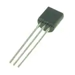
Case: E-Line (TO-92 Compatible)
Case Material: Molded Plastic, “Green” Molding Compound.
Flammability Classification Rating 94V-0
Moisture Sensitivity: Level 1 per J-STD-020
Terminals: Matte Tin Finish
Weight: 0.159 grams (approximate)
UL
D
G
S
E-Line
Equivalent Circuit
Pin Out - Bottom View
Ordering Information (Note 1)
Part Number
ZVN4306ASTZ
ZVN4306A
Notes:
Package
E-Line
E-Line
Marking
ZVN4306A
ZVN4306A
Quantity
2,000 per Ammo pack
4,000 loose per box
1. Diodes, Inc. defines “Green” products as those which are RoHS compliant and contain no halogens or antimony compounds. All applicable RoHS
exemptions applied. Further information about Diodes Inc.’s “Green” Policy can be found on our website at http:// www.diodes.com
Marking Information
ZVN4306A = Product Type Marking Code On Rounded Face
ZVN4306A
Document number: DS33367 Rev. 4 - 2
1 of 6
www.diodes.com
January 2012
© Diodes Incorporated
�A Product Line of
Diodes Incorporated
ZVN4306A
Maximum Ratings @TA = 25°C unless otherwise specified
Characteristic
Drain-Source Voltage
Gate-Source Voltage
Continuous Drain Current
Practical Continuous Drain Current
Pulsed Drain Current
Thermal Characteristics
Value
60
±20
1.1
1.3
15
Unit
V
V
A
A
A
Value
850
1.13
150
111
50
-55 to +150
Unit
mW
W
°C/W
°C/W
°C/W
°C
@TA = 25°C unless otherwise specified
Characteristic
Power Dissipation
Practical Power Dissipation
Thermal Resistance, Junction to Ambient
Thermal Resistance, Junction to Ambient
Thermal Resistance, Junction to Leads
Operating and Storage Temperature Range
Notes:
Symbol
VDSS
VGSS
ID
IDP
IDM
(Note 2)
(Note 2)
(Note 3)
Symbol
PD
PDP
RθJA
RθJA
RθJL
TJ, TSTG
2. For a device mounted on 25mm X 25mm X 1.6mm FR-4 PCB with high coverage of single sided 1oz copper, in still air condition.
3. Thermal resistance from junction to solder-point
ZVN4306A
Document number: DS33367 Rev. 4 - 2
2 of 6
www.diodes.com
January 2012
© Diodes Incorporated
�A Product Line of
Diodes Incorporated
ZVN4306A
Electrical Characteristics @TA = 25°C unless otherwise specified
Characteristic
OFF CHARACTERISTICS (Note 4)
Drain-Source Breakdown Voltage
Symbol
Min
Typ
Max
Unit
BVDSS
60
-
V
Zero Gate Voltage Drain Current TJ = 25°C
IDSS
-
-
Gate-Source Leakage
On-State Drain Current
ON CHARACTERISTICS (Note 4)
Gate Threshold Voltage
IGSS
ID(on)
12
-
1
20
±100
-
VGS(th)
1.3
Static Drain-Source On-Resistance
RDS (on)
-
gfs
700
0.22
0.32
-
3
0.33
0.45
-
mS
Ciss
Coss
Crss
td(on)
tr
td(off)
tf
-
-
350
140
30
8
25
30
16
pF
pF
pF
ns
ns
ns
ns
Forward Transconductance
DYNAMIC CHARACTERISTICS (Note 4)
Input Capacitance
Output Capacitance
Reverse Transfer Capacitance
Turn-On Delay Time (Note 5)
Turn-On Rise Time (Note 5)
Turn-Off Delay Time (Note 5)
Turn-Off Fall Time (Note 5)
Notes:
µA
nA
A
V
Ω
Test Condition
VGS = 0V, ID = 1mA
VDS = 60V, VGS = 0V
VDS = 48V, VGS = 0V, TA = 125°C
VGS = ±20V, VDS = 0V
VGS = 10V, VDS = 10V
VDS = VGS, ID = 1mA
VGS = 10V, ID = 3A
VGS = 5V, ID = 1.5A
VDS = 10V, ID = 3A
VDS = 25V, VGS = 0V,
f = 1.0MHz
VDD = 25V, ID = 3A, VGEM = 10V
4. Measured under pulsed conditions. Width = 300µs. Duty cycle ≤ 2%
5. Switching times measured with 50Ω source impedance and
很抱歉,暂时无法提供与“ZVN4306A”相匹配的价格&库存,您可以联系我们找货
免费人工找货