P-CHANNEL ENHANCEMENT
MODE VERTICAL DMOS FET
ZVP2106A
ISSUE 2 – MARCH 94
FEATURES
* 60 Volt VDS
* RDS(on)=5Ω
ID(On) -On-State Drain Current (Amps)
ID(On) -On-State Drain Current (Amps)
TYPICAL CHARACTERISTICS
-3.5
VGS=
-20V
-18V -14V
-3.0
-2.5
-12V
-2.0
-10V
-1.5
-9V
-8V
-1.0
-7V
-6V
-0.5
-5V
-4V
0
0
-10
-20
-30
-40
-50
-2.0
-1.8
VGS=
-10V
-1.6
-1.4
-1.2
-9V
-1.0
-8V
-0.8
-7V
-0.6
-6V
-0.4
-5V
-4V
-3.5V
-0.2
0
0
VDS - Drain Source Voltage (Volts)
VDS-Drain Source Voltage (Volts)
-8
-6
-4
ID=
-1A
-2
-0.5A
-0.25A
0
-2
-4
-6
-8
-10
-1.0
VDS=-10V
-0.8
-0.6
-0.4
PARAMETER
SYMBOL
VALUE
UNIT
Drain-Source Voltage
V DS
-60
V
Continuous Drain Current at T amb=25°C
ID
-280
mA
Pulsed Drain Current
I DM
-4
A
Gate Source Voltage
V GS
± 20
V
Power Dissipation at T amb=25°C
P tot
700
mW
Operating and Storage Temperature Range
T j :T stg
-55 to +150
°C
PARAMETER
SYMBOL MIN.
Drain-Source Breakdown
Voltage
BV DSS
-60
Gate-Source Threshold
Voltage
V GS(th)
-1.5
MAX. UNIT CONDITIONS.
V
I D=-1mA, V GS=0V
-3.5
V
ID=-1mA, V DS= V GS
-0.2
0
-2
-4
-6
-8
-10
Gate-Body Leakage
I GSS
20
nA
V GS=± 20V, V DS=0V
Zero Gate Voltage Drain
Current
I DSS
-0.5
-100
µA
µA
V DS=-60 V, V GS=0
V DS=-48 V, V GS=0V, T=125°C (2)
On-State Drain Current(1)
I D(on)
A
V DS=-18 V, V GS=-10V
5
Ω
V GS=-10V,I D=-500mA
mS
V DS=-18V,I D=-500mA
-1
Static Drain-Source On-State R DS(on)
Resistance (1)
Forward Transconductance
(1)(2)
2.6
-2.0
ID-Drain Current (Amps)
On-resistance v drain current
ABSOLUTE MAXIMUM RATINGS.
ELECTRICAL CHARACTERISTICS (at Tamb = 25°C unless otherwise stated).
-1.2
-7V -8V -9V -10V
-1.0
2.4
2.2
n)
(o
DS
2.0
1.8
1.6
1.4
Dr
1.2
1.0
Gate Thresh
old
0.8
0.6
eR
nc
ta
sis
e
eR
rc
ou
-S
n
ai
VGS=-10V
ID=-0.5A
VGS=VDS
ID=-1mA
Voltage VGS
(th
)
-40 -20
0
20 40 60 80 100 120 140 160 180
Tj-Junction Temperature (°C)
Normalised RDS(on) and VGS(th) vs Temperature
3-418
S
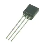
E-Line
TO92 Compatible
VGS-Gate Source Voltage (Volts)
5
1
-0.1
D
G
-10
Transfer Characteristics
Normalised RDS(on) and VGS(th)
RDS(ON) -Drain Source Resistance (Ω)
-6V
-8
-1.4
VGS-Gate Source Voltage (Volts)
VGS=-5V
-6
-1.6
Voltage Saturation Characteristics
10
-4
Saturation Characteristics
ID(On)-On-State Drain Current (Amps)
Output Characteristics
0
-2
VDS - Drain Source Voltage (Volts)
-10
ZVP2106A
g fs
150
Input Capacitance (2)
C iss
100
pF
Common Source Output
Capacitance (2)
C oss
60
pF
Reverse Transfer
Capacitance (2)
C rss
20
pF
Turn-On Delay Time (2)(3)
t d(on)
7
ns
Rise Time (2)(3)
tr
15
ns
Turn-Off Delay Time (2)(3)
t d(off)
12
ns
Fall Time (2)(3)
tf
15
ns
V DS=-18V, V GS=0V, f=1MHz
V DD ≈-18V, I D=-500mA
(1) Measured under pulsed conditions. Width=300µs. Duty cycle ≤2%
(2) Sample test.
3-417
Switching times measured with 50Ω source impedance and
很抱歉,暂时无法提供与“ZVP2106ASTZ”相匹配的价格&库存,您可以联系我们找货
免费人工找货- 国内价格
- 1+3.76920
- 10+3.06720
- 30+2.72160
- 100+2.37600
- 国内价格
- 10+7.18110
- 200+4.28370
- 500+2.99860
- 2000+2.14190
- 4000+2.03480
- 20000+1.88480
- 国内价格
- 1+2.56300
- 100+1.98000
- 1000+1.71600
- 2000+1.63900
- 国内价格 香港价格
- 2000+4.005522000+0.51704
- 4000+3.706724000+0.47847
- 6000+3.554536000+0.45882
- 10000+3.3835510000+0.43675
- 14000+3.2823214000+0.42369
- 20000+3.2033120000+0.41349