ZXFV203EV
ZXFV201EV
TRIPLE AND QUAD CHANNEL VIDEO AMPLIFIER EVALUATION BOARD
Evaluation board description
Power supply filtering
The wide bandwidth of the ZXFV201/3 quad/triple
channel video amplifiers necessitates some care in the
layout of the printed circuit. For this reason Zetex has
made available an Evaluation Board.
For the power supply filtering, low inductance surface
mount capacitors are normally required. It has been
found that very good RF decoupling is provided on
each supply using a 1000pF NPO size 0805 or smaller
ceramic surface mount capacitor, closest to the device
pin, with an adjacent 0.1µF X7R capacitor. Other
configurations are possible and it may be found that a
single 0.01uF X7R capacitor on each supply gives good
results. However this should be supported by larger
decoupling capacitors elsewhere on the printed circuit
board. Values of 1 to 10 µF are recommended
particularly where the voltage regulators are located
more than a few inches from the device. These larger
capacitors are recommended to be solid tantalum
electrolytic or ceramic types.
The evaluation board layout serves as a useful
example for many applications, showing a practical
implementation of the advice given below.
Figures 1, 2, 3 and 4 show the schematic and copper
layout of a double-sided printed circuit board suitable
for evaluation of the device in the laboratory.
BNC connector sockets allow connection to test
instruments via 50⍀ cables. The output circuit includes
a resistor matching circuit to present a load of 150⍀ to
the amplifier (equivalent to a 75⍀ back-terminated
video line) and simultaneously provide a 50⍀ output
impedance.
A parts list is provided below.
Evaluation board parts list
QTY
Cct Ref
1
Resistors, surface
3 (1) /4
R1 (2) R5
R12 R22
6 (1) /8
R2 (2) R3 (2)
R6 R7 R9
R10 R15
R16
3 (1) /4
R4 (2) R8
R11 R21
R13 R18 (2)
3 (1) /4
R19 R23
R14 R17 (2)
3 (1) /4
R20 R24
The attenuation of this matching circuit is 15.45 dB. As
the amplifier is configured for a voltage gain of 2, the
overall gain is:
6 - 15.45 = -9.45dB
PCB design
A continuous ground plane is required under the
device (except around its inverting input) to provide
the shortest possible ground return paths for signals
and power supply filtering.
A double-sided or multi-layer PCB construction is
required, with plated-through via holes providing
closely spaced low-inductance connections from some
components to the continuous ground plane (some of
these holes are not visible in the figures for the
Evaluation Board - artworks and NC drill output can be
provided if required).
Value Description
Printed circuit board ZDB189
mount
51R
Resistor chip
470R
Resistor chip
130R
Resistor chip
33R
Resistor chip
24R
Resistor chip
Capacitors, surface mount
2
C1,C2
100nF
2
C3,C4
-
C5-C8
Integrated circuits
1
U1
Miscellaneous
8
J1-J8
1
J9
2.2µF
Capacitor ceramic
chip X7R
Capacitor ceramic
chip X7R
NOT FITTED
ZXFV201 (3) /ZXFV203 (1)
Socket BNC, PCB square
flange
Terminal block, 3 way
NOTES:
(1) Applies to ZXFV203EV only
(2) Not present on ZXFV203EV
(3) Applies to ZXFV201EV only
ISSUE 1 - MARCH 2004
1
SEMICONDUCTORS
�SEMICONDUCTORS
J5
V-
GND
J1
J9:1
J9:2
J9:3
2
51R
R12
9
10
51R
R1
2
3
VCC
8
U1:C
V EE
ZXFV201
V EE
VCC
4
11
V+
470R
R10
470R
R9
2.2UF
C4
100NF
C2
ZXFV201
1
U1:A
100NF
C7
R2
130R
24R
R14
33R
R13
C5
J7
51R
R22
13
12
ZXFV201EV/ZXFV203EV schematic
J6
33R
R18
24R
130R
Figure 1
R1 1
470R
R3
470R
R17
R4
51R
6
C1
R5
5
J2
J3
2.2UF
C3
ZXFV201
14
U1:D
ZXFV201
7
U1:B
470R
R16
470R
R15
470R
R7
470R
R6
C8
C6
130R
R21
130R
R8
33R
R23
24R
R24
33R
R19
24R
R20
J8
J4
ZXFV203EV
ZXFV201EV
ISSUE 1 - MARCH 2004
�ZXFV203EV
ZXFV201EV
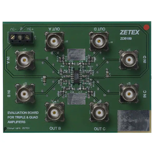
TOP VIEW
ZETEX
O UT A
O UT D
ZDB189
IND
IN A
INC
IN B
EVALUATION BOARD
FOR TRIPLE & QUAD
AMPLIFIERS
OUT B
Figure 2
OUT C
ZXFV201E/ZXFV203EV silkscreen
T OP VIEW
Figure 3
ZXFV201EV/ZXFV203EV top copper
ISSUE 1 - MARCH 2004
3
SEMICONDUCTORS
�ZXFV203EV
ZXFV201EV
T OP VIEW
Figure 4
ZXFV201EV/ZXFV203EV bottom copper
© Zetex plc 2004
Europe
Americas
Asia Pacific
Corporate Headquaters
Zetex GmbH
Streitfeldstraße 19
D-81673 München
Germany
Zetex Inc
700 Veterans Memorial Hwy
Hauppauge, NY 11788
USA
Zetex (Asia) Ltd
3701-04 Metroplaza Tower 1
Hing Fong Road, Kwai Fong
Hong Kong
Zetex plc
Fields New Road, Chadderton
Oldham, OL9 8NP
United Kingdom
Telefon: (49) 89 45 49 49 0
Fax: (49) 89 45 49 49 49
europe.sales@zetex.com
Telephone: (1) 631 360 2222
Fax: (1) 631 360 8222
usa.sales@zetex.com
Telephone: (852) 26100 611
Fax: (852) 24250 494
asia.sales@zetex.com
Telephone (44) 161 622 4444
Fax: (44) 161 622 4446
hq@zetex.com
These offices are supported by agents and distributors in major countries world-wide.
This publication is issued to provide outline information only which (unless agreed by the Company in writing) may not be used, applied or reproduced
for any purpose or form part of any order or contract or be regarded as a representation relating to the products or services concerned. The Company
reserves the right to alter without notice the specification, design, price or conditions of supply of any product or service.
For the latest product information, log on to
www.zetex.com
ISSUE 1 - MARCH 2004
SEMICONDUCTORS
4
�
很抱歉,暂时无法提供与“ZXFV201EV”相匹配的价格&库存,您可以联系我们找货
免费人工找货