ZXMD63C02X
20V DUAL N AND P-CHANNEL ENHANCEMENT MODE MOSFET
SUMMARY
N-CHANNEL: V(BR)DSS=20V; RDS(ON)=0.13V; ID=2.4A
P-CHANNEL: V(BR)DSS=-20V; RDS(ON)=0.27V; ID=-1.7A
DESCRIPTION
This new generation of high density MOSFETs from Zetex utilises a unique
structure that combines the benefits of low on-resistance with fast switching
speed. This makes them ideal for high efficiency, low voltage, power
management applications.
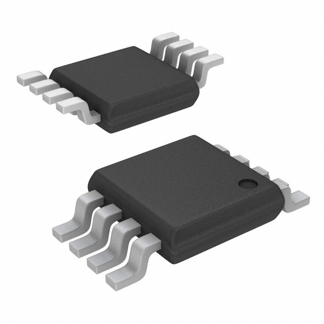
MSOP8
FEATURES
•
Low on-resistance
•
Fast switching speed
•
Low threshold
•
Low gate drive
•
Low profile SOIC package
N-CHANNEL
P-CHANNEL
APPLICATIONS
•
DC - DC Converters
•
Power Management Functions
•
Disconnect switches
•
Motor control
ORDERING INFORMATION
DEVICE
REEL SIZE
(inches)
TAPE WIDTH (mm)
QUANTITY
PER REEL
ZXMD63C02XTA
7
12mm embossed
1000 units
ZXMD63C02XTC
13
12mm embossed
4000 units
DEVICE MARKING
•
ZXM63C02
PROVISIONAL ISSUE A - JUNE 1999
1
Top View
�ZXMD63C02X
ABSOLUTE MAXIMUM RATINGS.
PARAMETER
SYMBOL
Drain-Source Voltage
V DSS
N-CHANNEL
P-CHANNEL
UNIT
20
-20
V
-1.7
-1.35
A
± 12
V
Gate- Source Voltage
V GS
Continuous Drain Current (V GS=4.5V; T A=25°C)(b)(d)
(V GS=4.5V; T A=70°C)(b)(d)
ID
Pulsed Drain Current (c)(d)
I DM
19
-9.6
A
Continuous Source Current (Body Diode)(b)(d)
IS
-1.5
-1.4
A
I SM
19
Pulsed Source Current (Body Diode)(c)(d)
2.4
1.9
-9.6
A
Power Dissipation at T A=25°C (a)(d)
Linear Derating Factor
PD
0.87
6.9
W
mW/°C
Power Dissipation at T A=25°C (a)(e)
Linear Derating Factor
PD
1.04
8.3
W
mW/°C
Power Dissipation at T A=25°C (b)(d)
Linear Derating Factor
PD
1.25
10
W
mW/°C
Operating and Storage Temperature Range
T j:T stg
-55 to +150
°C
THERMAL RESISTANCE
PARAMETER
SYMBOL
VALUE
UNIT
Junction to Ambient (a)(d)
R θJA
143
°C/W
Junction to Ambient (b)(d)
R θJA
100
°C/W
Junction to Ambient (a)(e)
R θJA
120
°C/W
NOTES
(a) For a device surface mounted on 25mm x 25mm FR4 PCB with high coverage of single sided 1oz copper,
in still air conditions
(b) For a device surface mounted on FR4 PCB measured at t
很抱歉,暂时无法提供与“ZXMD63C02XTC”相匹配的价格&库存,您可以联系我们找货
免费人工找货- 国内价格 香港价格
- 4000+5.123054000+0.66135