ZXSC400
LED DRIVER BOOST CONVERTER
DESCRIPTION
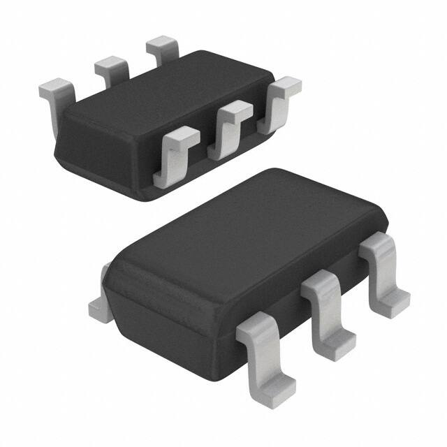
The ZXSC400 is a voltage mode boost converter in the SOT23-6 package. Its low
feedback voltage allows the current in a chain of LEDs to be set and accurately
monitored with a single resistor giving minimal losses. Its excellent load and line
regulation means that for the full supply range from lithium-ion cells, the LED
current will typically change by less than 1%. Using high efficiency Zetex switching
transistors with ratings of 20V and higher allow many LEDs to be chained in series
for the best LED current matching possible.
FEATURES
SOT23-6
• 1.8V to 8V supply range
• Typical output regulation of ⫾1%
• Over 80% typical efficiency
• 4.5A typical shutdown current
• Series connection for ultimate LED current matching
APPLICATIONS
• White LED backlighting for colour LCD panels
• General LED backlighting
• High performance white LED flashlights
PINOUT
• General LED driving from batteries
ORDERING INFORMATION
DEVICE
REEL
SIZE
TAPE
WIDTH
QUANTITY
PER REEL
7“
8mm
3000 units
ZXSC400E6TA
VCC
GND
DRIVE
VFB
STDN
SENSE
Top View
DEVICE MARKING
• C400
ISSUE 1 - JANUARY 2003
1
�ZXSC400
ABSOLUTE MAXIMUM RATINGS
VCC
DRIVE
EOR
STDN
SENSE
Operating Temp.
Storage Temp.
Power Dissipation
-0.3V to
-0.3V to
-0.3V to
-0.3V to
-0.3V to
-40°C to
-55°C to
450mW
+10V
VCC + 0.3V
VCC + 0.3V
The lower of (+5.0V) or (VCC + 0.3V)
The lower of (+5.0V) or (VCC + 0.3V)
+85°C
+125°C
ELECTRICAL CHARACTERISTICS
Test Conditions VCC= 3V, T= -40°C to 85°C unless otherwise stated.
Symbol
Parameter
Conditions
Limits
Min
Typ
Units
Max
Supply parameters
V IN
V CC Range
Iq 1
Quiescent Current
I STDN
Shutdown Current
Eff 1
Efficiency
30mA > I LED > 10mA
Acc REF
Reference tolerance
1.8V < V CC < 8V
TCO REF
Reference Temp Co
T DRIVE
Discharge pulse width
F OSC
Operating Frequency
1.8
8
V CC = 8V
220
A
4.5
80
-3.0
%
3.0
0.005
1.8V < V CC < 8V
V
A
%
%/⬚C
s
1.7
200
kHz
Input parameters
V SENSE
Sense voltage
I SENSE
Sense input current
V FB
Feedback voltage
2
V FB = 0V, V SENSE = 0V
22
28
34
mV
-1
-7
-15
A
291
300
309
mV
-1.2
-4.5
A
V IH
Shutdown high voltage
1.5
VCC
V
V IL
Shutdown low voltage
0
0.55
V
dV LN
Line voltage regulation
I FB
Feedback input current
V FB = 0V, V SENSE = 0V
0.5
%/V
Output parameters
I OUT 3
Output current
Vin > 2V, Vout = 10.5V
I DRIVE
Transistor drive current
Vdrive = 0.7V
2
V DRIVE
Transistor voltage drive
1.8V < V CC < 8V
0
C DRIVE
Mosfet gate drive cpbty
dILD 4
Load current regulation
50
mA
3.5
5
V C C -0.4
300
mA
V
pF
0.1
mA/V
Note
1
2
3
4
Excluding gate/base drive current.
IFB is typically half these values at 300mV.
System not device spec, including recommended transistors. 10.5V represents 3 white LEDs.
Change in LED current with changing supply voltage (LED VF x number of series LEDs).
ISSUE 1 - JANUARY 2003
2
�ZXSC400
TYPICAL CHARACTERISTICS
ISSUE 1 - JANUARY 2003
3
�ZXSC400
DESIGN INFORMATION
IC operation description
Block diagram
Bandgap Reference
All threshold voltages and internal currents are
derived from a temperature compensated bandgap
reference circuit with a reference voltage of 1.22V
nominal.
Dynamic Drive Output
Depending on the input signal, the output is either
“LOW” or “HIGH”. In the high state a 2.5mA current
source (max drive voltage = VCC-0.4V) drives the base
or gate of the external transistor. In order to operate
the external switching transistor at optimum
efficiency, both output states are initiated with a short
transient current in order to quickly discharge the base
or the gate of the switching transistor.
2µs
Switching Circuit
The switching circuit consists of two comparators,
Comp1 and Comp2, a gate U1, a monostable and the
drive output. Normally the DRIVE output is “HIGH”; the
external switching transistor is turned on. Current
ramps up in the inductor, the switching transistor and
external current sensing resistor. This voltage is
sensed by comparator, Comp2, at input ISENSE. Once
the current sense voltage across the sensing resistor
exceeds 30mV, comparator Comp2 through gate U1
triggers a re-triggerable monostable and turns off the
output drive stage for 2s. The inductor discharges to
the load of the application. After 2s a new charge
cycle begins, thus ramping the output voltage. When
the output voltage reaches the nominal value and FB
gets an input voltage of more than 300mV, the
monostable is forced “on” from Comp1 through gate
U1, until the feedback voltage falls below 300mV. The
above action continues to maintain regulation.
Pin functions
Pin No.
Name
Description
1
V CC
Supply voltage, 1.8V to 8V.
2
GND
Ground
3
STDN
Shutdown
4
SENSE
Inductor current sense input. Internal threshold voltage set to 30mV. Connect
external sense resistor
5
V FB
Reference voltage. Internal threshold set to 300mV. Connect external resistor
to program LED current
6
DRIVE
Drive output for external switching transistor. Connect to base or gate of
external switching transistor.
ISSUE 1 - JANUARY 2003
4
�ZXSC400
APPLICATIONS INFORMATION
Switching transistor selection
Capacitor Selection
The choice of switching transistor has a major impact
on the converter efficiency. For optimum performance,
a bipolar transistor with low VCE(SAT) and high gain is
required. The VCEO of the switching transistor is also an
important parameter as this sees the full output
voltage when the transistor is switched off. Zetex
SuperSOT™ transistors are an ideal choice for this
application.
A small value, low ESR ceramic capacitor is required to
filter the output, typically 1F to 4.7F.
Schottky diode selection
The inductor value must be chosen to satisfy
performance, cost and size requirements of the overall
solution.
Generally an input capacitor is not required, but a small
ceramic capacitor may be added to aid EMC, typically
1F to 4.7F.
Inductor Selection
As with the switching transistor, the Schottky rectifier
diode has a major impact on the converter efficiency. A
Schottky diode with a low forward voltage and fast
recovery time should be used for this application.
Inductor selection has a significant impact on the
converter performance. For applications where
efficiency is critical, an inductor with a series resistance
of 250m⍀ or less should be used.
The diode should be selected so that the maximum
forward current rating is greater or equal to the
maximum peak current in the inductor, and the
maximum reverse voltage is greater or equal to the
output voltage. The Zetex ZHCS Series meet these
needs.
A list of recommended inductors is listed in the table
below:
Combination devices
To minimise the external component count Zetex
recommends the ZX3CDBS1M832 combination of
NPN transistor and Schottky diode in a 3mm x 2mm
MLP package. This device is recommended for use in
applications using 1 to 4 white LEDs.
The IC is also capable of driving MOSFETs. Zetex
recommends the ZXMNS3BM832 combination of low
threshold voltage N-Channel MOSFET and Schottky
diode in a 3mm x 2mm MLP package. This device is
recommended for use in applications using 1 to 8 white
LEDs.
Part No.
Manufacture
L
I PK (A)
R DC ( )
CMD4D11-100MC
Sumida
10H
0.5
0.457
CMD4D11-220MC
Sumida
22H
0.4
0.676
LPO2506OB-103
Coilcraft
10H
1.0
0.24
ST2006103
Standex Electronics Inc
10H
0.6
0.1
ISSUE 1 - JANUARY 2003
5
�ZXSC400
Peak current definition
Programming LED current
In general, the IPK value must be chosen to ensure that
the switching transistor, Q1, is in full saturation with
maximum output power conditions, assuming
worse-case input voltage and transistor gain under all
operating temperature extremes.
Once the required output power is determined, the LED
current can be programmed by adding a single resistor
in the LED chain. The resistor value is determined by
the following:
Once I PK is decided the value of R SENSE can be
determined by:
RSENSE =
VSENSE
IPK
Sense Resistor
A low value sense resistor is required to set the peak
current. Power in this resistor is negligible due to the
low sense voltage threshold, VISENSE. At the bottom of
the page there is a table of recommended sense
resistors.
Output power calculation
ILED =
By making the above assumptions for inductance and
peak current the output power can be determined by:
Where VFB = 300mV
POUT = IAV x VIN x (Watts)
RLED selection table
VFB
RLED
where
IAV =
IPK
(TON + TDIS)
×
2
(TON + TOFF)
and
TON
IPK × L
=
VIN
and
TDIS =
IPK × L
(VLED − VIN)
RLED
40mA
7.5⍀
30mA
10⍀
20mA
15⍀
15mA
20⍀
10mA
30⍀
Shutdown Control
The ZXSC400 offers a shutdown mode that consumes
a standby current of less than 5A. When the voltage at
the STDN pin between 1V and 8V (and also open circuit),
the ZXSC400 is enabled and the driver is in normal
operation. When the voltage at the STDN pin is 0.7V or
lower, the ZXSC400 is disabled and the driver is in
shutdown mode. The SHDN input is a high impedance
current source of 1A typ. The driving device can be an
open collector or an open drain or a logic output with a
“High“ voltage of 5V max. The device shutdown
current depends of the supply voltage, see typical
characteristics graph
and
TOFF ≅ 1.7s (internally set by ZXSC400)
and
= efficiency e.g. 100% = 1
Operating frequency can be derived by:
F =
ILED
1
TON + TOFF
Manufacture
Series
RDC( ) Range
Size
Tolerance
URL
Cyntec
RL1220
0.022 - 10
0805
±5%
www.cyntec.com
IRC
LR1206
0.010 - 1.0
1206
±5%
www.irctt.com
ISSUE 1 - JANUARY 2003
6
�ZXSC400
Open-circuit protection
Dimming Control using the shutdown pin
For applications where the LED chain might go
open-circuit a Zener diode can be connected across the
LED chain preventing over-voltage and possible
damage to the main switching transistor. The Zener
diodes should be selected by ensuring its voltage
rating is higher than the combined forward voltage of
the LED chain. Under open circuit conditions the curren
in the Zener diode defines the output current as:
The first method uses the shutdown pin. By injecting a
PWM waveform on this pin and varying the duty cycle,
LED current and hence LED brightness can be adjusted.
IZ =
To implement this method of brightness control on the
ZXSC400, apply PWM signal with amplitude of
between 0.7V and Vcc at a frequency of 120Hz or above
(to eliminate LED flicker). The LED current and hence
LED brightness is linearly proportional to the duty cycle
ratio, so for brightness control adjust duty cycle ratio as
necessary. For example, a 10% duty cycle equates to
10% of full LED brightness.
VFB
RZ
The circuit example below give an open circuit output
current of 300A.
Dimming Control
There are four types of dimming control that can be
implemented for the ZXSC400.
ISSUE 1 - JANUARY 2003
7
�ZXSC400
Dimming Control using a DC voltage
Dimming Control using a logic signal
For applications where the shutdown pin is not
available a DC voltage can be used to control dimming.
By adding resistors R2 and R3 and applying a DC
voltage, the LED current can be adjusted from 100% to
0%. As the DC voltage increases, the voltage drop
across R2 increases and the voltage drop across R1
decreases, thus reducing the current through the LEDs.
Selection of R2 and R3 should ensure that the current
from the DC voltage is much less than the LED current
and much larger than the feedback current. The
component values in the diagram below represent 0%
to 100% dimming control from a 0 to 2V DC voltage.
For applications where the LED current needs to be
adjusted in discrete steps a logic signal can be applied
as shown in the diagram below. When Q1 os ‘off’, R1
sets the minimum LED current. When Q1 is ‘on’, R2 sets
the LED current that will be added to the minimum LED
current. The formula for selecting values for R1 and R2
are given below:
ZXSC400 VFB
R2
ZXSC400 VFB
VDC
R3
R2
67k
10k
LOGIC
SIGNAL
Q1
R1
R1
MOSFET ‘off’
VFB
ILED(MIN) =
RLEB
MOSFET ‘on’
VFLB
ILED(MAX) =
+ ILED(MIN)
RLEB
Dimming Control using a filtered PWM signal
The filtered PWM signal can be considered as an
adjustable DC voltage by applying a RC filter. The
values shown in the diagram below are configured to
give 0% to 100% dimming for a 1kHz to 100kHz PWM
signal with a 2V amplitude. e.g. a 50% duty cycle will
give 50% dimming.
Where VFB = 300mV
ZXSC400 VFB
PWM
R4
R3
R2
10k
67k
10k
R1
C1
0.1µF
ISSUE 1 - JANUARY 2003
8
�ZXSC400
Layout considerations
To optimise for best performance each of these loops
kept separate from each other and interconnected with
short, thick traces thus minimising parasitic
inductance, capacitance and resistance. Also the
RSENSE resistor should be connected, with minimum
trace length, between emitter lead of Q1 and ground,
again minimising stray parasitics.
Layout is critical for the circuit to function in the most
efficient manner in terms of electrical efficiency,
thermal considerations and noise.
For ‘step-up converters’ there are four main current
loops, the input loop, power-switch loop, rectifier loop
and output loop. The supply charging the input
capacitor forms the input loop. The power-switch loop
is defined when Q1 is ‘on’, current flows from the input
through the inductor, Q1, RSENSE and to ground. When
Q1 is ‘off’, the energy stored in the inductor is
transferred to the output capacitor and load via D1,
forming the rectifier loop. The output loop is formed by
the output capacitor supplying the load when Q1 is
switched back off.
ISSUE 1 - JANUARY 2003
9
�ZXSC400
REFERENCE DESIGNS
Li - Ion to 2 LED converter
30
100
Efficiency (%)
90
Load Current (mA)
2 White LEDs
ILED=20mA
80
70
60
2.5
3.0
3.5
2 White LEDs
25
20
15
10
5
0
4.0
2.5
Input voltage (V)
3.0
3.5
4.0
Input Voltage (V)
Input Voltage vs Efficiency
Input Voltage vs LED Current
Bill of Materials
Ref
Value
U1
U2
Part Number
Manufacture
Comments
ZXSC400
Zetex
LED driver IC
ZX3CDBS1M832
Zetex
NPN + Schottky dual
L1
10H
CMD4D11-100MC
Sumida
1mm height profile
R1
100m⍀
LR1206 / RL1220
IRC / Cyntec
1206 / 0805 size
R2
15⍀
Generic
Generic
0603 size
C1
2.2F/6V3
GRM Series
Murata
0805 size
C2
2.2F/16V
GRM Series
Murata
1206 size
NSCW215
Nichia
White SMT LED
LED
ISSUE 1 - JANUARY 2003
10
�ZXSC400
Li - Ion to 3 LED converter
90
30
3 White LEDs
3 White LEDs
ILED=20mA
LED Current (mA)
Efficiency (%)
100
80
70
60
2.5
3.0
3.5
20
10
0
2.5
4.0
3.0
3.5
4.0
Input Voltage (V)
Input Voltage (V)
Input Voltage v Efficiency
Input Voltage v LED Current
Bill of Materials
Ref
Value
U1
U2
Part Number
Manufacture
Comments
ZXSC400
Zetex
LED driver IC
ZX3CDBS1M832
Zetex
NPN + Schottky dual
L1
10H
CMD4D11-100MC
Sumida
1mm height profile
R1
68m⍀
LR1206 / RL1220
IRC / Cyntec
1206 / 0805 size
R2
15⍀
Generic
Generic
0603 size
C1
2.2F/6V3
GRM Series
Murata
0805 size
C2
2.2F/16V
GRM Series
Murata
1206 size
NSCW215
Nichia
White SMT LED
LED
ISSUE 1 - JANUARY 2003
11
�ZXSC400
Li - Ion to 4 LED converter
90
30
80
L=22µH
RSENSE=80mΩ
Load Current (mA)
Efficiency (%)
4 White LEDs
ILED=20mA
L=10µH
RSENSE=47mΩ
70
60
2.5
3.0
3.5
20
15
10
5
0
4.0
4 White LEDs
25
2.5
Input voltage (V)
3.0
3.5
4.0
Input Voltage (V)
Input Voltage vs Efficiency
Input Voltage vs LED Current
Bill of Materials
Ref
Value
U1
U2
Part Number
Manufacture
Comments
ZXSC400
Zetex
LED driver IC
ZX3CDBS1M832
Zetex
NPN + Schottky dual
L1
10H
CMD4D11-100MC
Sumida
1mm height profile
R1
47m⍀
LR1206 / RL1220
IRC / Cyntec
1206 / 0805 size
R2
15⍀
Generic
Generic
0603 size
C1
2.2F/6V3
GRM Series
Murata
0805 size
C2
2.2F/16V
GRM Series
Murata
1206 size
NSCW215
Nichia
White SMT LED
LED
ISSUE 1 - JANUARY 2003
12
�ZXSC400
Li - Ion to 6 LED converter
90
30
Load Current (mA)
Efficiency (%)
6 White LEDs
ILED=20mA
80
70
60
2.5
3.0
3.5
20
15
10
5
0
4.0
6 White LEDs
25
2.5
Input voltage (V)
3.0
3.5
4.0
Input Voltage (V)
Input Voltage vs Efficiency
Input Voltage vs LED Current
Bill of Materials
Ref
Part Number
Manufacture
Comments
U1
Value
ZXSC400
Zetex
LED driver IC
Q1
FMMT619
Zetex
40V NPN
D1
ZHCS1000
Zetex
1A Schottky diode
L1
22H
CMD4D11-220MC
Sumida
1mm height profile
R1
47m⍀
LR1206 / RL1220
IRC / Cyntec
1206 / 0805 size
R2
15⍀
Generic
Generic
0603 size
C1
2.2F/6V3
GRM Series
Murata
0805 size
C2
2.2F/25V
GRM Series
Murata
1206 size
NSCW215
Nichia
White SMT LED
LED
ISSUE 1 - JANUARY 2003
13
�ZXSC400
Li - Ion to 8 LED converter
90
30
Load Current (mA)
Efficiency (%)
8 White LEDs
ILED=20mA
80
70
60
2.5
3.0
3.5
8 White LEDs
25
20
15
10
5
0
2.5
4.0
Input voltage (V)
3.0
3.5
4.0
Input Voltage (V)
Input Voltage vs Efficiency
Input Voltage vs LED Current
Bill of Materials
Ref
Part Number
Manufacture
Comments
U1
ZXSC400
Zetex
LED driver IC
Q1
FMMT619
Zetex
40V NPN
D1
ZHCS1000
Zetex
1A Schottky diode
22H
CDRH4D28-220
D01608C-223
Sumida
Coilcraft
0.7A, 0.235⍀
0.7A, 0.37⍀
L1
or
Value
R1
33m⍀
LR1206 / RL1220
IRC / Cyntec
1206 / 0805 size
R2
15⍀
Generic
Generic
0603 size
C1
2.2F/6V3
GRM Series
Murata
0805 size
C2
2.2F/35V
GRM Series
Murata
1206 size
NSCW215
Nichia
White SMT LED
LED
ISSUE 1 - JANUARY 2003
14
�ZXSC400
Notes
ISSUE 1 - JANUARY 2003
15
�ZXSC400
PACKAGE OUTLINE
PAD LAYOUT DETAILS
e
b
L 2
E1
E
DATUM A
a
e1
D
C
A
A2
A1
CONTROLLING DIMENSIONS IN MILLIMETRES APPROX CONVERSIONS INCHES.
PACKAGE DIMENSIONS
Millimetres
Inches
DIM
Millimetres
Inches
DIM
Min
Max
Min
Max
Min
Max
Min
Max
A
0.90
1.45
0.35
0.057
E
2.60
3.00
0.102
0.118
A1
0.00
0.15
0
0.006
E1
1.50
1.75
0.059
0.069
A2
0.90
1.30
0.035
0.051
L
0.10
0.60
0.004
0.002
b
0.35
0.50
0.014
0.019
e
0.95 REF
0.037 REF
C
0.09
0.20
0.0035
0.008
e1
1.90 REF
0.074 REF
D
2.80
3.00
0.110
0.118
L
0°
10°
0°
10°
© Zetex plc 2003
Americas
Asia Pacific
Zetex GmbH
Streitfeldstraße 19
D-81673 München
Zetex Inc
700 Veterans Memorial Hwy
Hauppauge, NY11788
Germany
Telefon: (49) 89 45 49 49 0
Fax: (49) 89 45 49 49 49
europe.sales@zetex.com
USA
Telephone: (631) 360 2222
Fax: (631) 360 8222
usa.sales@zetex.com
Zetex (Asia) Ltd
3701-04 Metroplaza, Tower 1
Hing Fong Road
Kwai Fong
Hong Kong
Telephone: (852) 26100 611
Fax: (852) 24250 494
asia.sales@zetex.com
Europe
Zetex plc
Fields New Road
Chadderton
Oldham, OL9 8NP
United Kingdom
Telephone (44) 161 622 4422
Fax: (44) 161 622 4420
uk.sales@zetex.com
These offices are supported by agents and distributors in major countries world-wide.
This publication is issued to provide outline information only which (unless agreed by the Company in writing) may not be used, applied or reproduced
for any purpose or form part of any order or contract or be regarded as a representation relating to the products or services concerned. The Company
reserves the right to alter without notice the specification, design, price or conditions of supply of any product or service.
For the latest product information, log on to
www.zetex.com
ISSUE 1 - JANUARY 2003
16
�


 工商网监
湘ICP备2023018690号
工商网监
湘ICP备2023018690号
