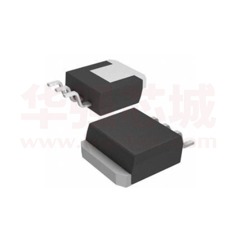
BL1084
5A LOW DROPOUT LINEAR REGULATOR
Outline:
Features:
BL1084 is a series of low dropout three
terminal regulators with a dropout of 1.4V at
5A load current.
● Other than a fixed version and an
adjustable version, output value can be
customized on command.
● Maximum output current is 5A
● Range of operation input voltage: Max
18V
● Line regulation: 0.2% (Typical)
● Load regulation: 0.2% (Typical)
● Environment Temperature: 0℃~80℃
Other than a fixed version (Vout =
1.8V,2.5V,3.3V,5.0V ) , BL1084 has an
adjustable version, The adjustable version can
set the output voltage with two external
resistors.
BL1084 offers thermal shut down and current
limit functions, to assure the stability
of chip and power system.
Applications:
:
The BL1084 series is available in standard
packages of TO-263-2L, TO-263-3L, TO-220
and TO-252.
● Power Management for Computer
Mother Board, Graphic Card
● Battery Charger
● Post Regulators for Switching Supplies
● Microprocessor Supply
Pin Configuration:
:
Marking
information:
:
A:
Means
Manufacture
weeks
B:
Means
Manufacture LOT
No.
C:
Means Output
Voltage Value
D:
Means Temp.
Range&Rohs Std
http://www.belling.com.cn
- 1Total 13 Pages
5/8/2007
�BL1084
:
Pin Description:
Fixed Version
Pin No.
1
2
3
Symbol
GND
Vout
Vin
Adjustable Version
Definition
Ground
Output
Input
Pin No.
1
2
3
Symbol Definition
Adj.
Adjustable
Vout
Output
Vin
Input
Ordering Information:
BL1084-XX X X
Package Type:
:
S:TO-263-2L
S1:TO-263-3L
Y:TO-252
Z:TO-220
Temp. Range & Rohs Std.:
:
C:80°C & Pb-free Rhos Std
Z:80°C & Pb/Sn Plating
Output Voltage:
:
18……1.8V
25……2.5V
33……3.3V
50……5.0V
Default:Adjustable Version
http://www.belling.com.cn
- 2Total 13 Pages
5/8/2007
�BL1084
Block Diagrams:
:
Absolute Maximum Ratings:
:
Maximum Input Voltage------------------------------------------------------------------------------- 18V
Junction Temperature (TJ)---------------------------------------------------------------------------- 150°C
Environment Temperature (TA) --------------------------------------------------------------------- 80°C
Storage Temperature (Ts)---------------------------------------------------------------------------- -65~150°C
Lead Temperature and Time ---------------------------------------------------------------------------------260°C,10S
Recommended Work Conditions:
:
Item
Min
Input Voltage Range
Environment Temperature
0
Recommended
Max
Unit
15
80
V
°C
Electrical Characteristics (Table 1):
:
Tj=25℃
Symbol
Vref
Vout
Parameter
Reference
Voltage
Output
Voltage
Conditions
Min
Typ
Max
Unit
Iout=10mA, Vin-Vout=3V
10mA≤Iout≤5A ,1.5V≤Vin-Vout≤5V
1.238
1.225
1.25
1.25
1.262
1.275
V
BL1084-1.80V
Iout=0mA,Vin=4.8V,Tj=25℃
10mA≤Iout≤5A ,3.4V≤Vin≤7V
1.782
1.764
1.80
1.80
1.818
1.836
2.475
2.45
2.50
2.50
2.525
2.55
BL1084-2.50V
Iout=0mA,Vin=5.5V,Tj=25℃
10mA≤Iout≤5A ,4.1V≤Vin≤7V
http://www.belling.com.cn
- 3Total 13 Pages
V
V
5/8/2007
�BL1084
∆Vout
∆Vout
Vin-Vout
BL1084-3.3V
Iout=0mA,Vin=6.3V,Tj=25℃
10mA ≤Iout≤5A ,4.9V≤Vin≤8V
3.267
3.234
3.3
3.3
3.333
3.366
V
BL1084-5.0V
Iout=0mA,Vin=8.0V,Tj=25℃
10mA ≤Iout≤5A ,6.6V≤Vin≤10V
4.95
4.90
5.0
5.0
5.05
5.10
V
BL1084-ADJ
Iout=10mA
2.85V≤Vin≤12V
0.035
0.2
%
BL1084-1.8V
Iout=10mA
3.4V≤Vin≤12V
7
15
mV
BL1084-2.5V
Iout=10mA
4.1V≤Vin≤12V
7
15
mV
BL1084-3.3V
Iout=10mA
4.9V≤Vin≤12V
7
15
mV
BL1084-5.0V
Iout=10mA
6.6V≤Vin≤12V
7
15
mV
BL1084-ADJ
Vin-Vout=3V, 10mA≤Iout≤5A
0.2
0.4
%
BL1084-1.8V
Vin-Vout=3V, 0≤Iout≤5A
16
30
mV
BL1084-2.5V
Vin-Vout=3V, 0≤Iout≤5A
16
30
mV
BL1084-3.3V
Vin-Vout=3V, 0≤Iout≤5A
16
30
mV
BL1084-5.0V
Vin-Vout=3V, 0≤Iout≤5A
16
30
mV
Dropout
Voltage
(note 3)
∆Vout, ∆Vref =1%,Iout=5A
1.4
V
Current Limit
Vin-Vout=3V, Tj=25℃
7
A
Minimum
Load Current
(note 4)
BL1084-ADJ
3
Line
Regulation
(note 1)
Load
Regulation
(note 1,2)
Ilimit
http://www.belling.com.cn
- 4Total 13 Pages
10
mA
5/8/2007
�BL1084
Iq
IAdj
Quiescent
Current
Adjust Pin
Current
(Adjustable
Version)
Ripple
Rejection
Ichange
θ JC
Vin=10V
5
10
mA
Vin=4.25V,
Iout=10mA
45
110
uA
F=120Hz,Cout=25uF( tan),
Iout=5A,Vin-Vout=3V
Adjust Pin
Current
Change
10mA≤Iout≤5A
1.5V≤Vin-Vout ≤6V
Temperature
Stability
Iout=10mA,
Vin-Vout=1.5V
Thermal
Resistance
junction to case
60
dB
0.2
TO-252
TO-263
TO-220
12.5
3
3
5
uA
0.5
%
℃/W
Note:
Note1:The Parameters of Line Regulation and Load Regulation in Table1 are tested under
constant junction temperature.
Note2: When Iout varies between 0~5A,Vin-Vout varies between 1.5V~6V under constant
junction temperature,the parameter is satisfied the criterion in table. If temperature
varies between 0℃≤TA≤80℃,it needs output current to be larger than 10mA to
satisfy the criterion.
Note3:Dropout Voltage is tested under Iout=5A and the following testing conditions: First step
is to find out the Vout value(Vout1) when Vin1=Vout+1.5V, second step is to decrease
Vin(Vin2) until Vout value is equal to 99%*Vout1(Vout2). Vdropout=Vin2-Vout2.
Note4:Minimum Load Current is defined as the minimum output current required to maintain
regulation. When 1.5V≦Vin-Vout≦6V,the device is guaranteed to regulate if the
output current is greater than 10mA.
Detailed Description:
BL1084 is a series of low dropout voltage, three terminal regulators. Its application circuit is very
simple: the fixed version only needs two capacitors and the adjustable version only needs two
resistors and two capacitors to work. It is composed of some modules including start-up circuit, bias
circuit, bandgap, thermal shutdown, current limit, power transistors and its driver circuit and so on.
The thermal shut down and current limit modules can assure chip and its application system
working safety when the environment temperature is larger than 80℃ or output current is larger than
5.2A.
The bandgap module provides stable reference voltage, whose temperature coefficient is
compensated by careful design considerations. The temperature coefficient is under 100ppm/℃.
And the accuracy of output voltage is guaranteed by trimming technique.
http://www.belling.com.cn
- 5Total 13 Pages
5/8/2007
�BL1084
Typical Application :
BL1084 has an adjustable version and fixed versions, Chart1 is its typical application:
BL1084
BL1084
Typical Application of BL1084
Application Hints:
1. Recommend using 10uF tan capacitor as bypass capacitor for all application circuit.
2. Recommend using 22uF tan capacitor to assure circuit stability.
3. Using a bypass capacitor(CAdj) between the adjust terminal and ground can improve ripple
rejection, This bypass capacitor prevents ripple from being amplified as the output voltage is
increased. The impedance of CAdj should be less than the resistor’s(R1) which is between output and
adjust pins to prevent ripple from being amplified at any ripple frequency. As R1 is normally in the
range of 120Ω~200Ω,the value of CAdj should satisfy this equation: 1/(2π*Fripple*Cadj)
