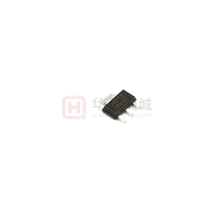
BL8071
1.5A Linear Regulator
GENERAL DESCRIPTION
FEATURES
BL8071 series are a group of positive voltage
output, high precise, and low power consumption
voltage regulator. Voltages are selectable in 100mV
steps within a range of 1.2V to 5.0V. It also can be
customized on command.
BL8071 series have excellent load and line
transient response and good temperature
characteristics, which can assure the stability of
chip and power system. And it uses trimming
technique to guarantee output voltage accuracy
within ±2%.
APPLICATIONS
BL8071 series are available in SOT-223 package,
which are lead (Pb)- free.
BL8071
LC1459
IN Cin
www.belling.com.cn
GND
VOUT
Reference Voltage Source
Battery Powered Equipment
PC Peripherals
Wireless Devices
Instrumentation
BLOCK DIAGRAM
TYPICAL APPLICATION
VDD
Low Quiescent Current: 100uA at 5V
High PSRR: 70dB range to 1KHz
Low Output Noise: 44uVRMS
Low Dropout: 300mV at 1A load
Maximum output current: 1.5A
Highly Accurate: ±2%
Low ESR Ceramic Capacitor Compatible
OUT
Cout
1
BL8071
ORDERING INFORMATION
PIN CONFIGURATION
BL8071 □
1□
2□
3□
4□
5
Code
Product Classification
JB:Product
Code
XX:Output
Voltage
JBXX
LLBYW A: A type
LL:LOT NO.
B:FAB Code
YW:Date Code
Product Classification
JB:Product
Code
XX:Output
Voltage
JBXX
LLBYW B: B type
LL:LOT NO.
B:FAB Code
YW:Date Code
□1
□2
□3
□4
□5
Description
Temperature&Rohs:
C:-40~85C ,Pb Free Rohs Std.
Package type:
LA: SOT-223 (A)
LB: SOT-223 (B)
Packing type:
TR:Tape&Reel (Standard)
Output voltage:
e.g. 12=1.2V 18=1.8V
25=2.5V 33=3.3V
50=5.0V
Voltage accuracy:
1=±1%(Customized)
Blank(default)=±2%
VDD
GND
VOUT
BL8071CLATR□□
BL8071CLBTR□□
Supply Voltage Input
Ground Pin
Output Voltage
Y: The Year of manufacturing,”1” stands for year 2011,
“2” stands for year 2012, and “8” stands for year 2018.
W: The week of manufacturing. ”A” stands for week
1,”Z” stands for week 26,” A ” stands for week 27,” Z ”
stands for week 52.
www.belling.com.cn
2
BL8071
ABSOLUTE MAXIMUM RATING
Parameter
Value
Max Input Voltage
Operating Junction Temperature (TJ)
Ambient Temperature (TA)
Package Thermal Resistance
Storage Temperature (TS)
Lead Temperature & Time
8V
125C
-40C~85C
20C / W
-40C~150C
260C, 10 Sec
SOT-223
Note:Exceed these limits to damage to the device.
Exposure to absolute maximum rating conditions may affect device reliability.
RECOMMENDED WORK CONDITIONS
Parameter
Value
Input Voltage Range
Ambient Temperature
Max. 6V
-40C~85C
ELECTRICAL CHARACTERISTICS
Test Conditions: CIN=4.7uF,COUT=4.7uF,TA=25C, unless otherwise specified.
Symbol
Parameter
VDD
Input Voltage
VOUT
Output
Voltage
VOUT>1.5
VOUT