BL8076
2A 3MHz 6V Synchronous Buck Converter
DESCRIPTION
FEATURES
The BL8076 is a high efficiency synchronous, buck
DC/DC converter. Its input voltage range is from
2.6V to 6V and provides an adjustable regulated
output voltage from 0.6V to Vin while delivering
up to 2A of output current.
The internal synchronous switches increase
efficiency and eliminate the need for an external
Schottky diode. It runs at a fixed 3MHz frequency,
which allows the use of small inductor with
L2000V
Note: Exceed these limits to damage to the device. Exposure to absolute maximum rating
conditions may affect device reliability.
www.belling.com.cn
2
�BL8076
RECOMMENDED WORK CONDITIONS
Parameter
Value
Input Voltage Range
Operating Junction Temperature(Tj)
Max. 6V
-20C –125C
ELECTRICAL CHARACTERISTICS
(VIN=5V, TA=25C)
Symbol
Parameter
VDD
UVLO
Vref
Ifblk
Input Voltage Range
Input Under Voltage Lockout
Feedback Voltage
Feedback Leakage current
Iq
Conditions
Line Regulation
Load Regulation
Switching Frequency
PMOS Rdson
RdsonN
Ilimit
Iswlk
Venh, Vmdh
Venl, Vmdl
Ienlk, Imdlk
Rdischarge
Typ
2.6
2.1
0.588
Increase Vin
Vin=5V, Ven=5V
2.2
0.6
0.01
30
0.1
0.04
0.15
3
100
Active, Vfb=0.65V, No Switching
Shutdown
Vin=2.7V to 5.5V
Iout=0.1 to 2A
Quiescent Current
LnReg
LdReg
Fsoc
RdsonP
Min
2.4
Isw=200mA
NMOS Rdson
Peak Current Limit
SW Leakage Current
EN/MODE High Threshold
EN/MODE Low Threshold
EN/MODE Leakage Current
Discharge Resistance
Isw=200mA
Unit
6.0
V
V
V
uA
uA
uA
%/V
%/A
MHz
mohm
0.612
0.1
1
3.6
120
80
3
2.5
Max
100
Vout=5.5V, EN=GND
mohm
A
uA
V
V
uA
Ohm
10
1.5
0.4
EN=MODE=GND
EN=GND
180
1
450
300
TYPICAL PERFORMANCE CHARACTERISTICS
(Vin=3.6V, L=1uH, Cin=10uF, Cout=10uF, TA=25C, unless otherwise stated)
Efficiency at Vout=1.8V
100%
100.00%
90%
90.00%
80%
80.00%
70%
70.00%
60%
60.00%
Efficiency
Efficiency
Efficiency at Vout=3.3V
50%
40%
50.00%
40.00%
30%
VIN=3.7V
30.00%
VIN=5.0V
20%
VIN=4.2V
20.00%
VIN=3.0V
10%
VIN=5.0V
10.00%
VIN=3.6V
0%
0.00%
0.0
0.5
1.0
1.5
2.0
2.5
0.0
www.belling.com.cn
0.5
1.0
1.5
Iout(A)
Iout(A)
3
2.0
2.5
�BL8076
Efficiency at Vout=1.2V
Load Regulation at Vout=1.8V
2
100.00%
1.95
90.00%
1.9
70.00%
1.85
60.00%
1.8
Vout (V)
Efficiency
80.00%
50.00%
40.00%
30.00%
1.75
1.7
1.65
VIN=3.0V
20.00%
VIN=3.6V
1.6
10.00%
VIN=5.0V
1.55
0.00%
0.0
0.5
1.0
1.5
2.0
VIN=3V
VIN=3.6V
VIN=5V
1.5
2.5
0
Iout(A)
Switching waveform Vin=3.6V, Vout=1.2V Iout=0A
0.5
1
1.5
2
2.5
Iout(A)
Switching waveform Vin=3.6V, Vout=1.2V Iout=0.7A
SW
SW
VOUT
VOUT
I_inductor
I_inductor
Switching waveform Vin=5V, Vout=3.3V, Iout=0A
Switching waveform Vin=5V, Vout=3.3V, Iout=0.5A
SW
SW
VOUT
VOUT
I_inductor
I_inductor
www.belling.com.cn
4
�BL8076
Load Transient
Vin=3.6V, Vout=1.2V, Iout=0.2A/1A
Load Transient
Vin=3.6V, Vout=1.8V, Iout=0.2A/1.5A
SW
SW
VOUT
VOUT
I_inductor
I_inductor
FUNCTIONAL DECRIPTIONS
The BL8076 high efficiency switching regulator is a small, simple, DC-to-DC step-down converter capable of delivering up
to 2A of output current. The device operates in pulse-width modulation (PWM) at 3MHz from a 2.6V to 5.5V input
voltage and provides an output voltage from 0.6V to VIN, making the BL8076 ideal for on-board post-regulation
applications. An internal synchronous rectifier improves efficiency and eliminates the typical Schottky free-wheeling
diode. Using the on resistance of the internal high-side MOSFET to sense switching currents eliminates current-sense
resistors, further improving efficiency and cost.
Loop Operation
BL8076 uses a PWM current-mode control scheme. An open-loop comparator compares the integrated voltage-feedback
signal against the sum of the amplified current-sense signal and the slope compensation ramp. At each rising edge of the
internal clock, the internal high-side MOSFET turns on until the PWM comparator terminates the on cycle. During this
on-time, current ramps up through the inductor, sourcing current to the output and storing energy in the inductor. The
current mode feedback system regulates the peak inductor current as a function of the output voltage error signal.
During the off cycle, the internal high-side P-channel MOSFET turns off, and the internal low-side N-channel MOSFET
turns on. The inductor releases the stored energy as its current ramps down while still providing current to the output.
Current Sense
An internal current-sense amplifier senses the current through the high-side MOSFET during on time and produces a
proportional current signal, which is used to sum with the slope compensation signal. The summed signal then is
compared with the error amplifier output by the PWM comparator to terminate the on cycle.
Current Limit
There is a cycle-by-cycle current limit on the high-side MOSFET. When the current flowing out of SW exceeds this limit,
the high-side MOSFET turns off and the synchronous rectifier turns on. BL8076 utilizes a frequency fold-back mode to
prevent overheating during short-circuit output conditions. The device enters frequency fold-back mode when the FB
voltage drops below 200mV, limiting the current to IPEAK and reducing power dissipation. Normal operation resumes
upon removal of the short-circuit condition.
Soft Start
BL8076 has a internal soft-start circuitry to reduce supply inrush current during startup conditions. When the device
exits under-voltage lockout (UVLO), shutdown mode, or restarts following a thermal-overload event, the l soft-start
circuitry slowly ramps up current available at SW.
www.belling.com.cn
5
�BL8076
UVLO and Thermal Shutdown
If VIN drops below 2V, the UVLO circuit inhibits switching. Once VIN rises above 2.1V, the UVLO clears, and the soft-start
sequence activates. Thermal-overload protection limits total power dissipation in the device. When the junction
temperature exceeds TJ= +160°C, a thermal sensor forces the device into shutdown, allowing the die to cool. The
thermal sensor turns the device on again after the junction temperature cools by 15°C, resulting in a pulsed output
during continuous overload conditions. Following a thermal-shutdown condition, the soft-start sequence begins.
DESIGN PROCEDURE
Inductor Selection
The peak-to-peak ripple is limited to 30% of the
maximum output current. This places the peak current
far enough from the minimum overcurrent trip level to
ensure reliable operation while providing enough current
ripples for the current mode converter to operate stably.
In this case, for 2A maximum output current, the
maximum inductor ripple current is 667 mA. The
inductor size is estimated as following equation:
LIDEAL=(VIN(MAX)-VOUT)/IRIPPLE*DMIN*(1/FOSC)
Output Capacitor Selection
For most applications a nominal 10μF or 22μF
capacitor is suitable. The BL8076 internal
compensation is designed for a fixed corner
frequency that is equal to
FC=
= 50Khz
For example, for VOUT=1.8V, L=1μH, COUT=10μF, for VOUT
=1.2V, L=0.47μH, COUT=22μF
Setting Output Voltage
Output voltages are set by external resistors. The FB_
threshold is 0.6V.
RTOP = RBOTTOM x [(VOUT / 0.6) - 1]
Therefore,
for VOUT=1.8V,
The inductor values is calculated to be L = 0.60μH.
Choose 1μH
Guidelines for Input Capacitor and Output Capacitor
The input capacitor in a DC-to-DC converter reduces
current peaks drawn from the battery or other input
power source and reduces switching noise in the
controller. The impedance of the input capacitor at
the switching frequency should be less than that of
the input source so high-frequency switching currents
do not pass through the input source. The output
capacitor keeps output ripple small and ensures
control-loop stability. The output capacitor must also
have low impedance at the switching frequency.
Ceramic, polymer, and tantalum capacitors are
suitable, with ceramic exhibiting the lowest ESR and
high-frequency impedance. Output ripple with a
ceramic output capacitor is approximately as follows:
VRIPPLE = IL(PEAK)[1 / (2π x fOSC x COUT)]
If the capacitor has significant ESR, the output ripple
component due to capacitor ESR is as follows:
VRIPPLE(ESR) = IL(PEAK) x ESR
And for VOUT =1.2V,
The inductor values is calculated to be L = 0.469μH.
Choose 0.47μH
The resulting ripple is
IRIPPLE =(VIN(MAX)-VOUT)/LACTUAL*DMIN*(1/FOSC)
When,
VOUT=1.8V, IRIPPLE = 403mA
VOUT=1.2V, IRIPPLE = 665mA
www.belling.com.cn
6
�BL8076
PACKAGE OUTLINE
Package
DFN2x2-8L
Package specification:
Devices per reel
3000pcs
Unit
mm
Package
Devices per reel
3000Pcs
Unit
mm
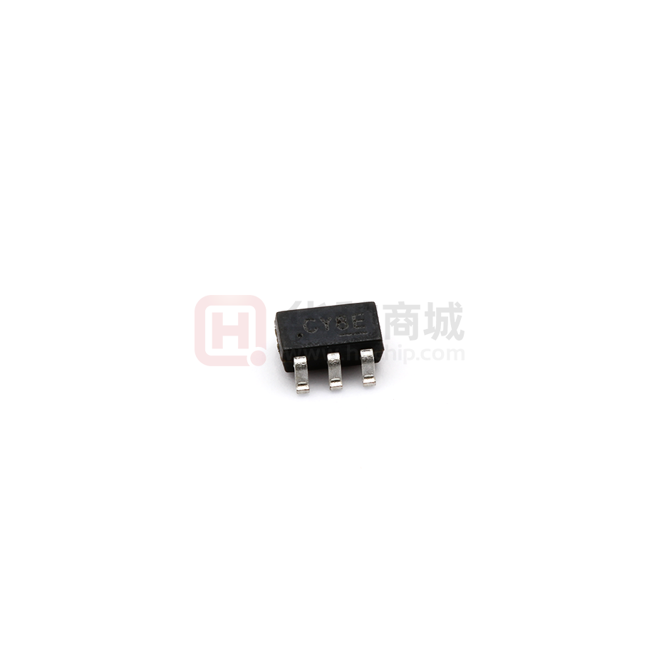
SOT-23-5
Package specification:
www.belling.com.cn
7
�