BL8531C
High Efficiency, Multi-Function Step-up DC/DC Controller
DESCRIPTION
FEATURES
BL8531C series are CMOS-based PFM step-up DCDC Controller with low supply current and high
output voltage accuracy. Quiescent current
drawn from power source is as low as 6uA. It is
capable of delivering 500mA output current at
4.0V output with 2V input Voltage. Only four
external components are necessary: An inductor,
a Schottky diode, an output filter capacitor and a
NMOSFET or a NPN transistor All of these
features make BL8531C series be suitable for the
portable devices, which are supplied by a single
battery to four-cell batteries.
BL8531C has a drive pin (EXT) for external
transistor. So it is possible to load a large output
current with a power transistor which has a low
voltage dropout.
BL8531C integrates stable reference circuits and
trimming technology, so it can afford high
precision and low temperature-drift coefficient of
the output voltage.
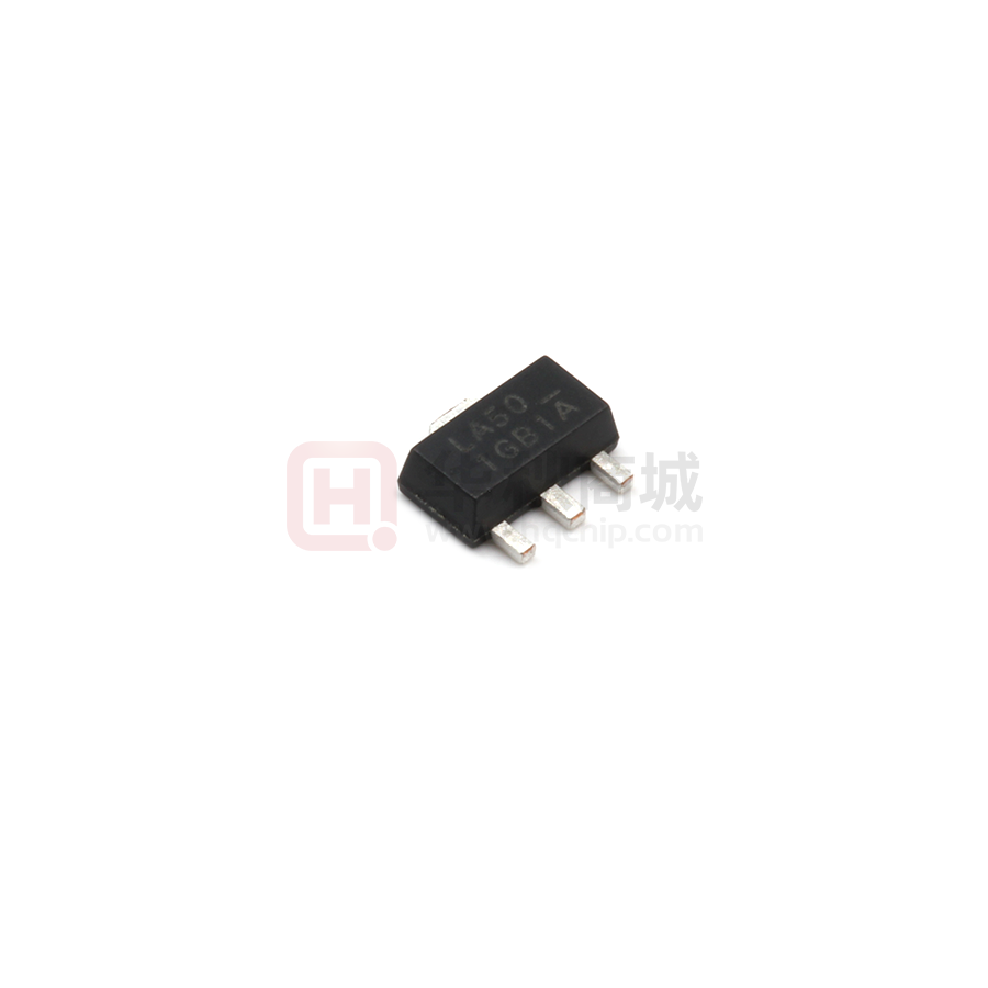
BL8531C is available in SOT-23-3, SOT-23-5 and
SOT-89-3 packages which are PB free. And in SOT23-5 the device can be switch on or off easily by
CE pin, to minimize the standby supply current.
Deliver 500mA at 4.0V Output voltage with
2V input Voltage
The controller output voltage can be adjusted
from 2.5V~6.0V(In 0.1V step)
Output voltage accuracy ---------------------2%
Low temperature-drift coefficient of the
output voltage-----------------------100ppm/C
Only four external components are necessary:
An inductor, a Schottky diode, an output filter
capacitor and a NMOSFET or a NPN transistor
High power conversion efficiency----------90%
Low quiescent current drawn from power
source--------------------------------------------- 6uA
Small package--SOT-23-3, SOT-23-5, SOT-89-3
APPLICATIONS
TYPICAL APPLICATION
Power source for PDA, DSC, MP3 Player,
electronic toy and wireless mouse
Power source for a single or dual-cell batterypowered equipments
Power source for LED
ELECTRICAL CHARACTERISTICS
BL8531C
www.belling.com.cn
1
�BL8531C
ORDERING INFORMATION
MARKING INFORMATION
BL8531C □
1□
2□
3□
4
Code
Product Classification
□
1
□
2
□
3
□
4
Description
Marking
3C:Product
Code
Temperature&Rohs:
C: -40~85C , Pb Free Rohs Std.
Package type:
B3: SOT-23-3
B5: SOT-23-5
C3: SOT-89-3
Packing type:
TR: Tape&Reel (Standard)
Output voltage:
e.g. 25=2.5V
56=5.6V
60=6.0V
3CXX
Parameter
Value
Output Voltage Range
EXT Pin Voltage
CE Pin Voltage
Operating Junction Temperature (Tj)
Ambient Temperature (Ta)
SOT-23-3
Power Dissipation
SOT-23-5
SOT-89-3
Storage Temperature (Ts)
Lead Temperature & Time
-0.3V-12V
-0.3V-(VOUT+0.3)
-0.3V-(VOUT+0.3)
125C
-40C -85C
250mW
250mW
500mW
-40C -150C
260C,10S
Note:
Exceed these limits to damage to the device.
Exposure to absolute maximum rating conditions may
affect device reliability.
Value
Suggestion: Use tantalum type capacitor to reduce the
ripple of the output voltage. Use 1nF filter ceramic
type capacitor to connect OUT pin and GND pin. The
filter capacitor is recommended as close as possible to
OUT pin and GND pin.
www.belling.com.cn
2
XX: Output
Voltage
Product Classification
LBXX
LLBYW
CE
GND
OUT
EXT
NC
RECOMMENDED WORK CONDITIONS
0.8V-Vout
10-100uH
≥10uF
47-220uF
-40C -85C
BL8531CCB3TR□ □
Marking
3C:Product
Code
3CXX
Parameter
XX: Output
Voltage
Product Classification
ABSOLUTE MAXIMUM RATING
Input Voltage Range
Inductor
Input Capacitor
Output Capacitor
Ambient Temperature (Ta)
BL8531CCB5TR□ □
BL8531CCC3TR□ □
Marking
LB: Product
Code
XX: Output
Voltage
LL: LOT NO.
B: FAB Code
YW: Date
Code
Chip Enable (Active high)
Ground Pin
Output Pin, Power supply for internal
Switching Pin
No Connection
�BL8531C
ELECTRICAL CHARACTERISTICS
Default condition (unless otherwise provided): Vin=0.6×Vout, Iout=10mA, Temperature=25C, Use external circuit in
test circuit list
SYMBOL
ITEM
Vout
Output Voltage
Vin
Iin
Input Voltage
Input Current *(No load)
IDD
Quiescent current *
Istandby
VCEH
VCEL
Chip leakage current
CE “H” threshold voltage
CE “L” threshold voltage
Fosc
Oscillator frequency
IEXTH
EXT”H” output current
IEXTL
EXT”L” output current
Duty
Oscillator duty cycle
TEST CONDITIONS
2.45
2.646
2.94
3.234
3.528
3.92
4.9
5.88
Iout=0mA, Vin=Vout*0.6
No external component,
Vout =Vout×1.05
VCE=0V
VCE: 02V
VCE: 20V
Vout=Vout*0.96
Test EXT pin frequency
3.0V
很抱歉,暂时无法提供与“BL8531CC3TR50”相匹配的价格&库存,您可以联系我们找货
免费人工找货- 国内价格
- 5+0.79900
- 20+0.72850
- 100+0.65800
- 500+0.58750
- 1000+0.55460
- 2000+0.53110
- 国内价格
- 5+1.02179
- 50+0.80234
- 150+0.70827
- 1000+0.59087
- 国内价格
- 1+0.74256
- 50+0.49504
- 1000+0.44800
- 国内价格
- 1+1.14710
- 10+0.84870
- 100+0.72740
- 1000+0.60620
