BL8536
0.9V startup, 1MHz, 300mA Iout, Low Iq, Synchronous Boost converter
DESCRIPTION
FEATURES
The BL8536 is a step-up converter that provides a
boosted output voltage from a low voltage
source. Because of its proprietary design, it starts
up at a very low input voltage down to 0.9V, and
only consumes 15uA at standby, making it an
ideal choice for single cell alkaline/NiMH battery
operations.
A switching frequency of 1MHz minimizes
solution footprint by allowing the use of tiny, low
profile inductors and ceramic capacitors. The
current mode PWM design is internally
compensated, reducing external parts count.
BL8536 is available in SOT23-3 and SOT89-3
Package.
Efficiency up to 94%@Vin=3.3V, Vout=5.5V
Typical 15uA standby current
1MHz Switching Frequency allows small
inductor and output cap
Input boost-strapping allows using small or
no input cap
Low Vin Start-up Voltage down to 0.9V Ideal
for Single Alkaline Cell operations
Maximum Output Current up to 300mA
Low Noise PWM control
Internally Compensated Current Mode Control
Internal Synchronous Rectifier
Available in SOT23-3 and SOT89-3
APPLICATIONS
TYPICAL APPLICATION
One to Three Cell Battery Operated Devices
Medical Instruments
Bluetooth Headsets
Flash-Based MP3 Players
Noise Canceling Headphones
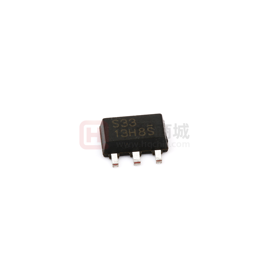
PIN OUT & MARKING
2.2uH
OUT
3
SW
VIN
SXX
LLHYW
SXYW
VOUT
OUT
10uF
BL8536
LC3500
1
GND
10uF
2
SW
SOT23-3
GND
S: Product Code
X: Output Voltage
YW: Date code
www.belling.com.cn
1
1
2
3
GND
OUT
SW
SOT89-3
S: Product Code
XX: Output Voltage
LL: LOT No.
H: FAB Code
YW: Date code
�BL8536
ORDERING INFORMATION
PART No.
PACKAGE
Tape&Reel
BL8536CB3TR
BL8536CC3TR
SOT23-3
SOT89-3
3000/Reel
1000/Reel
ABSOLUTE MAXIMUM RATING
Parameter
Value
SW Voltage
OUT Voltage
Max Operating Junction Temperature(Tj)
SOT23-3
Maximum Power Dissipation
SOT89-3
Ambient Temperature(Ta)
Storage Temperature(Ts)
Lead Temperature & Time
-0.3 ~ 6V
-0.3 ~ 6V
125C
450mW
500mW
-40C – 85C
-55C - 150C
260C, 10S
Note: Exceed these limits to damage to the device.
Exposure to absolute maximum rating conditions may affect device reliability.
ELECTRICAL CHARACTERISTICS
(TA=25C)
Symbol
Vin
Parameter
Conditions
Input Voltage Range
Min
Typ
0.9
Vstart
Startup Voltage
Iout = 1mA
0.9
Vhold
Hold Voltage
Iout = 50mA
0.5
Vout
Output Voltage Range
Fsoc
IQ
RdsonP
RdsonN
Iswlk
1.8
Max
Unit
5
V
V
0.7
V
5.5
V
Output voltage accuracy
Iout = 0mA
2
Line regulation
Iout = 50mA
0.1
0.2
%/V
Load regulation
Iout = 0~300mA
1
2
%
Switching Frequency
Vout=0.95Vo, No inductor
0.7
1
1.4
MHz
Max Duty cycle
Vout=0.95Vo, No inductor
85
90
95
%
Quiescent Current at Vout
Vout=1.05*Vo
5
8
15
uA
Supply current at Vin
Iout = 0mA
20
uA
Efficiency
PMOS Rdson
Iout = 100mA
Isw =100mA
NMOS Rdson
Isw =100mA
SW Leakage Current
Vout=5.2V, Vsw=0 or 5.2V
www.belling.com.cn
2
%
85
%
400
600
mohm
200
300
mohm
1
uA
�BL8536
PIN DESCRIPTION
PIN #
SOT23-3
3
1
2
SOT89-3
2
1
3
NAME
OUT
GND
SW
DESCRIPTION
Output voltage pin, with 10uF ceramic capacitor closely connected to GND
Ground
To connect inductor to VIN
BLOCK DIAGRAM
ELECTRICAL PERFORMANCE
Tested under Cin=Cout=10uF, L=2.2uH, TA=25C, unless otherwise specified
Efficiency vs. Output Current
Efficiency vs. Output Current
(Vout=3.3V)
100%
100%
90%
90%
80%
80%
70%
70%
60%
60%
Efficiency
Efficiency
(Vout=5.5V)
50%
40%
30%
10%
0%
0.001
0.01
0.1
Vin=1.0V
Vin=1.5V
Vin=2.0V
Vin=2.7V
20%
10%
1
Iout (A)
www.belling.com.cn
40%
30%
Vin=1.0V
Vin=1.5V
Vin=3.3V
Vin=4.0V
20%
50%
0%
0.001
0.01
0.1
Iout (A)
3
1
�BL8536
Efficiency vs. Output Current
100%
80%
80%
60%
60%
40%
Vin=1.0V
Vin=1.5V
Vin=2.0V
Vin=2.7V
20%
0%
0.001
0.01
0.1
Iout (A)
(Vout=1.8V)
100%
Efficiency
Efficiency
Efficiency vs. Output Current
(Vout=3.0V)
1
40%
0%
0.001
10
Output Voltage vs. Output Current
0.01
Iout (A)
0.1
1
Output Voltage vs. Output Current
(Vout=5.5V)
6.0
Vin=1.0V
Vin=1.2V
Vin=1.5V
20%
(Vout=3.3V)
4.0
3.5
5.0
3.0
Vout (V)
Vout (V)
4.0
3.0
2.0
Vin=1.0V
Vin=1.5V
Vin=3.3V
Vin=4.0V
1.0
0.0
0
0.2
0.4
Iout (A)
0.6
2.5
2.0
1.5
Vin=1.0V
Vin=1.5V
Vin=2.0V
Vin=2.7V
1.0
0.5
0.0
0.8
0
Output Voltage vs. Output Current
0.4
0.6
Iout (A)
0.8
1
Output Voltage vs. Output Current
(Vout=3.0V)
3.5
0.2
(Vout=1.8V)
2.0
3.0
1.5
2.0
Vout (V)
Vout (V)
2.5
1.5
Vin=1.0V
Vin=1.5V
Vin=2.0V
Vin=2.7V
1.0
0.5
0.0
0
0.2
0.4
0.6
0.8
Iout (A)
1
1.0
0.5
Vin=1.0V
Vin=1.2V
Vin=1.5V
0.0
1.2
0
Iq vs. Temperature
30
15
Vout(V)
Iq(uA)
20
10
5
0
-5
-50
www.belling.com.cn
0
50
Temperature(℃)
0.2
0.3
0.4
Iout (A)
0.5
0.6
Output Voltage vs. Temperature
Supply current at Vin
Quiescent Current at Vout
25
0.1
100
4
3.5
3.5
3.4
3.4
3.3
3.3
3.2
3.2
3.1
3.1
3.0
Vin=1.0V
Vin=2.6V
Vin=3.0V
-40
0
40
Temperature(℃)
80
120
�BL8536
DETAILED DESCRIPTION
APPLICATION INFORMATION
BL8536 is a low input voltage start up, current
mode DC-DC step up converter. It’s operation can
be best understood by referring to the block
diagram. Upon starting up, the low voltage startup
circuitry drives SW with on-off cycles, transferring
energy from input to OUT by storing energy in the
inductor during on-time and releasing it to the
output during off-time. When OUT reaches 2V, the
startup circuit turns off and the main controller
takes over. The main control loop consists of a
reference, a GM error amplifier, a PWM controller,
a current sense amplifier, an oscillator, a PWM logic
control, and it is power stage including its driver.
The main control loop is a classic current mode
control loop. The GM stage integrates the error
between FB and REF, and its output is used to
compare with a triangular wave which the summing
result of the current sense amplifier output and a
slope compensation voltage. The output of the
comparator is used to drive the power stage to
reach regulation.
Inductor selection
www.belling.com.cn
With switching frequency up to 1MHz, small surface
mount inductors can be used with values from
2.2uH to 4.7uH. For a given chosen inductor value
and application conditions make sure the peak
inductor current does not exceed the maximum
current rating of the selected vendor's inductor.
Input and output capacitor selection
The BL8536's bootstrap architecture allows the use
of very small input capacitor. For applications that
only need to drive small output load current, the
input capacitor is optional, because once output is
started up, the IC's is powered by OUT, a quiet
power supply.
The output capacitor is used to stabilize the loop
and provide ac current to the load. A low ESR
ceramic cap with values from 2.2uF to 22uF can be
used. Smaller value capacitors are generally
cheaper with small footprints, while larger
capacitor provides lower ripples and better
transient load responses. Also, when extreme low
startup voltage is needed, larger output capacitors
are needed for the part to startup under heavy load
condition.
5
�BL8536
PACKAGE OUTLINE
Package
SOT-23-3
Devices per reel
3000Pcs
Unit
mm
SOT-89-3
Devices per reel
1000Pcs
Unit
mm
Package dimension:
Package
Package dimension:
www.belling.com.cn
6
�
很抱歉,暂时无法提供与“BL8536CC3TR-3.3V”相匹配的价格&库存,您可以联系我们找货
免费人工找货- 国内价格
- 5+0.82943
- 20+0.77694
- 100+0.72444
- 500+0.67195
- 1000+0.64745
- 2000+0.62995