BL9110
1A Low Dropout, Low Quiescent Current
High PSRR CMOS Linear Regulator
FEATURES
⚫
PCMCIA Cards and Wireless LAN
⚫
Electrical appliances such as cameras, VCRS
⚫
Up to 1A Output Current
⚫
70uA Operating Supply Current
⚫
Excellent Line Regulation: 0.05%/V
⚫
Low Dropout: 350mV@1A(VOUT=3.3V)
the input voltage from 2.5V to 6V and delivers 1A
⚫
High Power Supply Rejection Ratio
load current. The BL9110 is available in two types,
⚫
Wide Operating Voltage Range: 2.5V to 6.0V
either fixed or adjustable output voltage. The output
⚫
1V to 5V Factory-Preset Output
voltage of the fixed types is preset at an internally
⚫
High Accuracy: ±1% or ±2%
trimmed voltage 1V, 1.2V, 1.3V, 1.5V, 1.8V, 2.5V,
⚫
Built-in Auto Discharge Function
2.7V, 2.8V, 2.85V, 3.0V, 3.2V, 3.3V, 5V or can be
⚫
500mA in-rush Current Limit
made with options of the output range from 1V to 5V
⚫
Fold-back Current Limit Protection
in 50mV increments. The output range of adjustable
⚫
Thermal Shutdown Protection
types is from 1V to 5V. The BL9110 consists of a
⚫
DFN-6,
⚫
SOT-89-5,
SOT-89-3,
DESCRIPTION
Step-Down
Converter
The BL9110 is a low-dropout regulator that operates
,
SOT-223-5,
voltage reference, an error amplifier, resistor net for
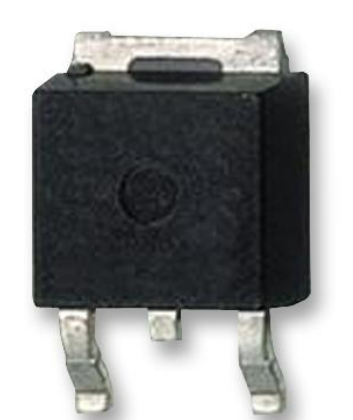
SOT-223-3, TO-263-3, TO-220-3, TO-252-3
setting output voltage, a current limit circuit for
and TO-252-5 Package
over-current and a thermal-shutdown circuit.
RoHS Compliant and 100% Lead (Pb)-Free
A standby mode with ultra low supply current can be
realized with the chip enable function. Since the
APPLICATIONS
packages for BL9110 are DFN-6, SOT-89-5,
⚫
Portable Communication Equipment
SOT-223-5,
⚫
Battery-Powered Equipment
SOT-89-3, TO-252-3, TO92-3 and TO-252-5 with
⚫
Laptop, Palmtops, Notebook Computers
high power dissipation, high density mounting of the
⚫
Hand-Held Instruments
IC on board is possible.
ORDERING INFORMATION
BL9110-VVV X X XX
Package:
AA: DFN-6
BA: SOT-89-5-A
CA: TO-252-5
DA: SOT-223-5
EA: TO-252-3-A
FA: SOT-223-3-A
FC: SOT-223-3-C
GA: TO-263-3-A
GC: TO-263-3-C
HA: TO-220-3
IA: SOT-89-3-A
IC: SOT-89-3-C
JA:TO92-3
SOT-223-3,
TO-263-3,
TO-220-3,
TYPICAL APPLICATION
BB: SOT-89-5-B
EB: TO-252-3-B
FB: SOT-223-3-B
FD: SOT-223-3-D
GB: TO-263-3-B
VDD
VDD
VOUT
VOUT
C1
10uF
C2
2.2uF
Chip
Enable
IB: SOT-89-3-B
BL9110
CE
GND
Features:
P: Standard (default, lead free)
C: Customized
Output Voltage Accuracy
A: ±1%
B: ±2%
Output Voltage
100:1.0V 120:1.2V 130:1.3V 150:1.5V
180:1.8V 250:2.5V 270:2.7V 280:2.8V
285:2.85V 300:3.0V 320:3.2V 330:3.3V
500:5.0V
ADJ: adjustable
www.belling.com.cn
Rev 2.2
Belling Proprietary Information. Unauthorized Photocopy and Duplication Prohibited
© 2011 Belling All Rights Reserved
1
�BL9110
1A Low Dropout, Low Quiescent Current
High PSRR CMOS Linear Regulator
Absolute Maximum Rating
Input Supply Voltage (VDD)
CE Input Voltage
Output Voltage
Output Current
(Note 1)
-0.3V to +7V
-0.3V to +7V
-0.3V to VIN+0.3V
1.4A
Maximum Junction Temperature
125°C
Operating Temperature Range (Note2) -40°C to 85°C
Storage Temperature Range
-65°C to 125°C
Lead
Temperature
(Soldering,
10s)
300°C
Step-Down Converter
,
Package Information
DFN-6
TOP VIEW
2
GND
3
VDD
NC/ADJ 1
5
VDD
GND
2
4
CE
CE
3
5
VOUT
CE 1
GND
4
VDD
TO-252-5
TOP VIEW
5
VOUT
4
VDD
MARKING
VOUT
6
MARKING
1
MARKING
VOUT
SOT-89-5
TOP VIEW
SOT-89-5
TOP VIEW
2
MARKING
NC/ADJ 3
3
2
1
VOUT GND GND
AA
BA
4
5
CE
VDD
BB
CA
Part Number
Top Mark
Temp Range
BL9110AA
BL9110-VVVXXAA
-40°C to +85°C
YWSS VVV (Note3)
BL9110BA/B
BL9110-VVVXXBA/B
-40°C to +85°C
YWSS VVV
BL9110CA
BL9110-VVVXXCA
-40°C to +85°C
YWSS VVV
TO-263-3
TOP VIEW
SOT-223-3
TOP VIEW
SOT-223-5
TOP VIEW
MARKING
MARKING
MARKING
1
2
3
VDD VOUT GND
4
5
ADJ
CE
FA
FB
FC
FD
1
1
2
3
VOUT
GND
GND
VDD
GND
VOUT
VDD
GND
VDD
VDD
VOUT
VOUT
GA
GB
GC
GND
GND
VDD
Part Number
Top Mark
Temp Range
BL9110-VVVXXDA
BL9110DA
-40°C to +85°C
www.belling.com.cn
Rev 2.2
Belling Proprietary Information. Unauthorized Photocopy and Duplication Prohibited
© 2011 Belling All Rights Reserved
2
3
VOUT
VDD
GND
2
VDD
VOUT
VOUT
�BL9110
1A Low Dropout, Low Quiescent Current
High PSRR CMOS Linear Regulator
YWSS VVV
BL9110EA/B
BL9110-VVVXXEA/B
-40°C to +85°C
YWSS VVV
BL9110FA/B/C/D
Step-Down
BL9110-VVVXXFA/B/C/D
Converter
YWSS VVV
BL9110GA/B/C
BL9110-VVVXXGA/B/C
DA
SOT-89-3
TOP VIEW
TO92
TOPVIEW
MARKING
MARKING
1
2
3
GND
GND
VOUT
VOUT
VDD
GND
VDD
VOUT
VDD
JA
HA
Part Number
Top Mark
BL9110-VVVXXJA
BL9110IA/B/C
3
GND
VOUT
VDD
-40°C to +85°C
YWSS VVV
BL9110JA
-40°C to +85°C
YWSS VVV
www.belling.com.cn
Rev 2.2
2
-40°C to +85°C
YWSS VVV
BL9110-VVVXXI/A/B/C
1
Temp Range
BL9110HA
BL9110-VVVXXHA
,
-40°C to +85°C
YWSS VVV
IA
IB
IC
-40°C to +85°C
Belling Proprietary Information. Unauthorized Photocopy and Duplication Prohibited
© 2011 Belling All Rights Reserved
3
�BL9110
1A Low Dropout, Low Quiescent Current
High PSRR CMOS Linear Regulator
Pin Descriptions
Symbol
Description
VOUT
Output Pin
GND
Ground Pin
CE
Chip Enable Pin (High active)
VDD
Input Pin
ADJ/NC
Adjustable/No Connection
Step-Down Converter
,
VVV
100
120
130
…
285
…
495
500
ADJ
Voltage (V)
1.0
1.2
1.3
…
2.85
…
4.95
5.0
Adjustable
Y
0
1
2
3
4
…
Year 2010 2011 2012 2013 2014 ……
W
Week
01
A
2
B
…
…
26
Z
27
28
…
…
52
Thermal Resistance (Note 4):
Package
ӨJA
ӨJC
DFN-6
95C/W
10C/W
SOT-89-5
160C/W
45C/W
TO-252-5
90C/W
10C/W
SOT-223-5
160C/W
20C/W
TO-252-3
90C/W
10C/W
SOT-223-3
160C/W
20C/W
TO-263-3
65C/W
7C/W
TO-220-3
50C/W
7C/W
SOT89-3
180C/W
50C/W
Note 1: Absolute Maximum Ratings are those values beyond which the life of a device may be impaired.
Note 2: The BL9110 is guaranteed to meet performance specifications from 0°C to 70°C. Specifications over the –40°C to
85°C operating temperature range are assured by design, characterization and correlation with statistical
process controls.
Note 3: Y: Year of assembly manufacturing
W: Week of assembly manufacturing
SS: Lot ID (the 7th and 8th number of Lot numbers)
VVV: Voltage code (for example 100 stands for 1.0V)
Note 4: Thermal Resistance is specified with approximately 1 square of 1 oz copper.
www.belling.com.cn
Rev 2.2
Belling Proprietary Information. Unauthorized Photocopy and Duplication Prohibited
© 2011 Belling All Rights Reserved
4
�BL9110
1A Low Dropout, Low Quiescent Current
High PSRR CMOS Linear Regulator
Block Diagram
Step-Down Converter
VDD
Voltage
Reference
-
Voltage
Buffer
EA
+
ADJ
Loop
Compensation
Fold-back
Current Limit
Over
Temperature
Protection
CE
,
Logic
Control
Power Good
Detector
VOUT
Soft-start
GND
www.belling.com.cn
Rev 2.2
Belling Proprietary Information. Unauthorized Photocopy and Duplication Prohibited
© 2011 Belling All Rights Reserved
5
�BL9110
1A Low Dropout, Low Quiescent Current
High PSRR CMOS Linear Regulator
Electrical Characteristics (Note 5)
BL9110-1.2V Electrical Characteristics
(VDD=2.5V, VOUT=1.2V, CE=VDD, CIN=10F, COUT=2.2F, TA=25°C, unless otherwise noted.)
Parameter
Symbol Step-Down
Conditions
MIN
TYP MAX
Converter
Input Voltage
VDD
2.5
6
-1
+1
IOUT=1mA
VOUT
Output Voltage Accuracy (Note 6)
-2
+2
Current Limit
ILIM
1.0
1.3
Short Circuit Current
ISCC
VOUT=0
250
Quiescent Current
IQ
IOUT=0mA
70
120
Standby Current
ISTBY
VCE=GND, Shutdown
0.01
1
IOUT=300mA
420
715
VDROP
Dropout Voltage (note 7)
IOUT=1A
870 1310
(Note
8)
ΔVLINE
2.5V≤VDD≤ 6V, IOUT=100mA
0.05
0.5
Line Regulation
(Note
9)
ΔV
1mA≤I
≤1A
20
Load Regulation
LOAD
OUT
IOUT=100mA
Output Voltage (Note 10)
TCVOUT
±100
-40°C≤T≤85°C
Temperature Coefficient
Logic Low
VIL
Shutdown
0.4
CE
Input Threshold
Logic High
VIH
Start up
1.0
CE Pull-down Resistance
RCE
5
Output Noise Voltage
eNO
10Hz to100KHz, IOUT=1mA
45
f=1kHz
70
(VOUT≤3.3V)
Power Supply
0.2VP-P Ripple
PSRR
Rejection Ratio
IOUT=100mA
f=1kHz
60
(VOUT>3.3V)
Thermal Shutdown Temperature
TSD
Shutdown, Temp increasing
165
Thermal Shutdown Hysteresis
TSDHY
30
Output Discharge Resistance
RDSC
50
unit
,V
%
A
mA
uA
uA
mV
%/V
mV
ppm/°C
V
V
MΩ
uVRMS
dB
°C
°C
Ω
Note 5: 100% production test at +25°C. Specifications over the temperature range are guaranteed by design and
characterization.
Note 6: This IC includes two kinds of output voltage accuracy versions. A: ±1%, B: ±2%.
Note 7: The required minimum input operating voltage is equal to V OUT+VDROP, and if VOUT+VDROP 3.3V)
Thermal Shutdown Temperature
TSD
Shutdown, Temp increasing
165
Thermal Shutdown Hysteresis
TSDHY
30
Output Discharge Resistance
RDSC
50
unit
V
%
,A
mA
uA
uA
mV
%/V
mV
ppm/°C
V
V
MΩ
uVRMS
dB
°C
°C
Ω
Note 5: 100% production test at +25°C. Specifications over the temperature range are guaranteed by design and
characterization.
Note 6: This IC includes two kinds of output voltage accuracy versions. A: ±1%, B: ±2%.
Note 7: The required minimum input operating voltage is equal to V OUT+VDROP, and if VOUT+VDROP