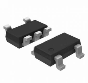
BL9162
300mA High PSRR, Ultra-low Noise,
Ultra-Fast CMOS LDO Regulator
FEATURES
Ultra-low Noise
Ultra-Fast Transient Response
High PSRR: -87dB @ 217Hz
-83dB @ 1KHz
-54dB @ 1MHz
0.1A Standby Current When Shutdown
Low Dropout: 140mV@300mA (VOUT=2.8V)
Wide Operating Voltage Ranges:
1.6V to 5.5V
Current Limiting and Short Circuit
Current Protection
Thermal Shutdown Protection
Only 1F Output Capacitor Required for
Stability
Fast output discharge
Available in SOT23-5, SC70-5 and
DFN1X1-4L Packages
APPLICATIONS
Cellular and Smart Phones
Cordless Telephones
Camera and Machine Vision Modules
Battery-Powered Equipment
Laptop, Palmtops, Notebook Computers
Hand-Held Instruments
PCMCIA Cards
Portable Information Appliances
DESCRIPTION
The BL9162 is designed for portable
applications with demanding performance
and space requirements. The BL9162
performance is optimized for battery-powered
systems to deliver ultra-low noise and low
quiescent current. Regulator ground current
increases only slightly in dropout, further
prolonging the battery life. The BL9162 also
works with low-ESR ceramic capacitors,
reducing the amount of board space
necessary for power applications, critical in
hand-held wireless devices. The BL9162
consumes only 0.1µA current in shutdown
mode and has fast turn-on time (Typical
100µs). The other features include ultra- low
dropout voltage, high output accuracy, current
limiting protection, and high ripple rejection
ratio.
TYPICAL APPLICATION
www.belling.com.cn
1
V1.5
�BL9162
300mA High PSRR, Ultra-low Noise,
Ultra-Fast CMOS LDO Regulator
ORDERING INFORMATION
Package Marking
SOT23-5 &SC70-5
DFN1×1-4L
V: Output voltage
Y: Data code—Year
W: Data code—Week
www.belling.com.cn
2
V1.5
�BL9162
300mA High PSRR, Ultra-low Noise,
Ultra-Fast CMOS LDO Regulator
V
Output Voltage
SOT23-5
V
Output Voltage
SC70-5 &
DFN1X1-4L
SOT23-5
SC70-5 &
DFN1X1-4L
1.0V
B
A
2.5V
E
P
1.05V
B
A
2.6V
T
Q
1.1V
F
B
2.8V
G
S
1.15V
F
B
3.0V
I
U
1.2V
A
C
3.3V
K
X
1.5V
C
F
3.6V
Y
Y
1.8V
D
I
4.0V
Z
Z
Y
4
5
6
…
0
1
…
Year
2014
2015
2016
…
2020
2021
…
W
A
…
Y
Z
a
…
y
z
Week
1
…
25
26
27
…
51
52
PIN CONFIGURATIONS
SOT23-5 & SC70-5
DFN1X1-4L
(TOP VIEW)
(TOP VIEW)
Thermal Resistance (Note 3)
ӨJA
ӨJC
SOT23-5
250℃/W
130℃/W
SC70-5
333℃/W
170℃/W
Package
www.belling.com.cn
3
V1.5
�BL9162
300mA High PSRR, Ultra-low Noise,
Ultra-Fast CMOS LDO Regulator
Pin Description
SOT23-5 & SC70-5
PIN
NAME
FUNCTION
1
VIN
Power Input Voltage.
2
3
4
5
GND
EN
NC
VOUT
Ground.
Chip Enable Pin, This pin has an internal pull-down resistor
No Connection.
Output Voltage.
DFN1X1-4L
PIN
NAME
FUNCTION
1
VOUT
Output Voltage.
2
3
4
Exposed
Pad
GND
EN
VIN
Ground.
Chip Enable Pin, This pin has an internal pull-down resistor
Power Input Voltage.
The exposed pad should be connected to a large ground plane to
maximize thermal performance.
Block Diagram
www.belling.com.cn
4
V1.5
�BL9162
300mA High PSRR, Ultra-low Noise,
Ultra-Fast CMOS LDO Regulator
Absolute Maximum Rating (Note 1)
Input Supply Voltage (VIN)
EN Pin Input Voltage
Output Voltages
Output Current
-0.3V to +6V
-0.3V to VIN
-0.3V to VIN+0.3V
300mA
Maximum Junction Temperature
150°C
(Note2)
Operating Temperature Range
-40°C to 85°C
Storage Temperature Range
-65°C to 125°C
Lead Temperature (Soldering, 10s)
300°C
Note 1: Absolute Maximum Ratings are those values beyond which the life of a device may be impaired.
Note 2: The BL9162 is guaranteed to meet performance specifications from 0°C to 70°C. Specifications over the –40°C to
85°C operating temperature range are assured by design, characterization and correlation with statistical process controls.
Note 3: Thermal Resistance is specified with approximately 1 square of 1 ozcopper.
www.belling.com.cn
5
V1.5
�BL9162
300mA High PSRR, Ultra-low Noise,
Ultra-Fast CMOS LDO Regulator
Electrical Characteristics (Note 4)
(VIN=Vout +1V, EN=VIN, CIN=COUT=1F, TA=25℃,unless otherwise noted.)
Parameter
Symbol
Input Voltage
VIN
Output Voltage Accuracy
VOUT
Current Limit
ILIM
RLOAD=1
Short Circuit Current
ISHORT
VOUT=0V
180
Quiescent Current
IQ
VEN>1.2V, IOUT=0mA
45
70
130
200
140
210
210
300
450
650
0.03
0.17
Dropout Voltage
VDROP
Conditions
VIN=Vout+1V,
IOUT=1mA
∆VLINE
∆VLOAD
1mA
很抱歉,暂时无法提供与“BL9162-180BARN”相匹配的价格&库存,您可以联系我们找货
免费人工找货