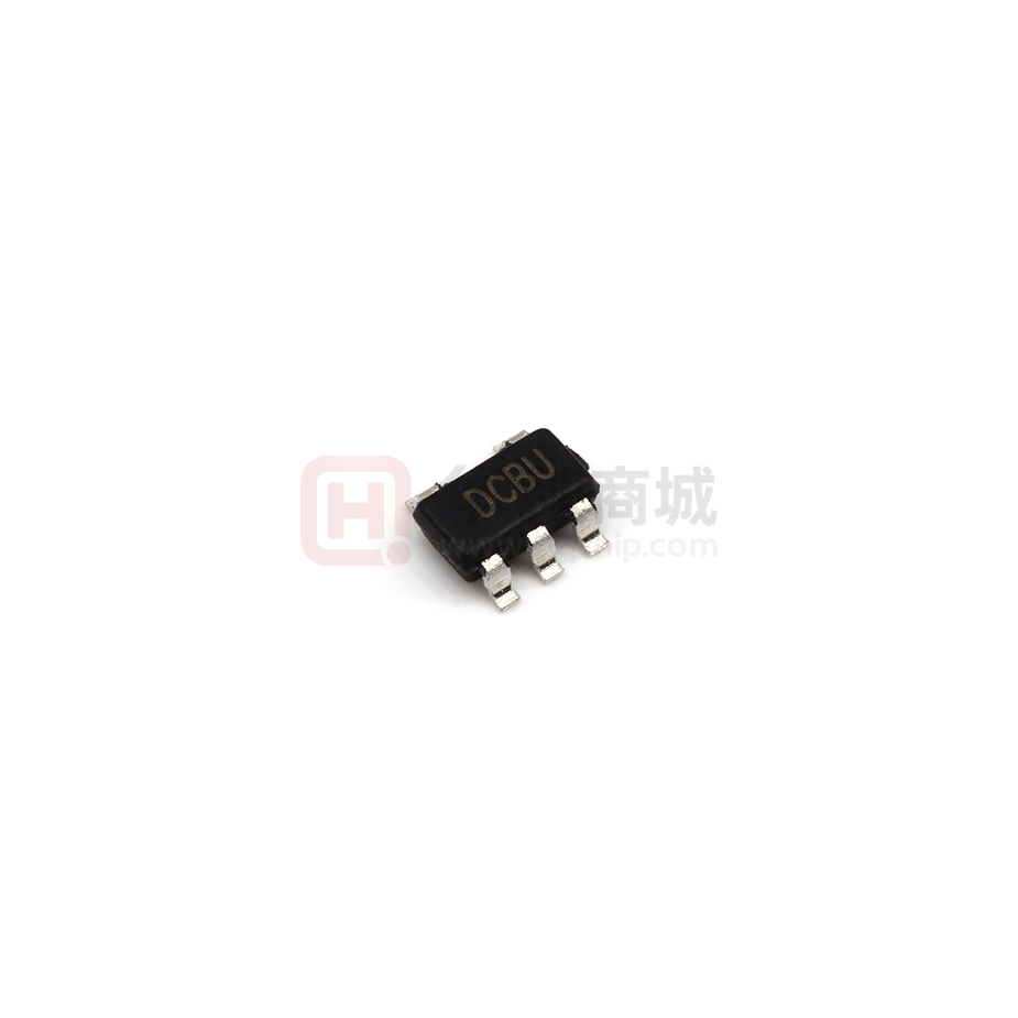
BL9198
300mA Ultra
tra-low Noise, Ultra
tra-Fast
CMOS LDO
LDO Regul
Regula
ulator
Hand-Held Instruments
PCMCIA Cards
MP3/MP4/MP5 Players
Portable Information Appliances
FEATURES
Ultra-low Noise for RF Application
Ultra-Fast Response in Line/Load
Transient
1.2V, IOUT=0mA
IOUT=200mA,
VOUT=2.8V
IOUT=300mA,
VOUT=2.8V
VIN=3.6V to 5.5V
IOUT=1mA
1mA
25mΩ on the BL9198 output ensures
stability. The BL9198 still works well with
output capacitor of other types due to the
wide stable ESR range. Output capacitor of
larger capacitance can reduce noise and
improve load transient response, stability,
and PSRR. The output capacitor should be
located not more than 0.5 inch from the
VOUT pin of the BL9198 and returned to a
clean analog ground.
Enable Function
The BL9198 features an LDO regulator enable/disable function. To assure the LDO
regulator will switch on; the EN turn on
control level must be greater than 1.2 volts.
The LDO regulator will go into the shut-
down mode when the voltage on the EN
pin falls below 0.4 volts. For to protect the
system, the BL9198 have a quick discharge function. If the enable function is
not needed in a specific application, it may
be tied to VIN to keep the LDO regulator in
a continuously on state.
Thermal Considerations
Thermal protection limits power dissipation
in BL9198. When the operation junction
temperature exceeds 165°C, the OTP
circuit starts the thermal shutdown function
turn the pass element off. The pass
element turns on again after the junction
temperature cools by 30°C.
For continue operation, do not exceed
absolute maximum operation junction
temperature 125°C. The power dissipation
definition in device is:
PD(MAX) = ( TJ(MAX) − TA ) /θJA
Where TJ(MAX) is the maximum operation
junction temperature 125°C, TA is the
ambient temperature and the θJA is the
junction to ambient thermal resistance. For
recommended operating conditions specification of BL9198, where TJ(MAX) is the
maximum junction temperature of the die
(125°C) and TA is the maximum ambient
temperature. The junction to ambient thermal resistance (θJA is layout dependent)
for SOT-23-5 package is 250°C/W, SC-705 package is 333°C/W, on
standard
JEDEC 51-3 thermal test board. The maximum power dissipation at TA= 25°C can
be calculated by following formula:
PD(MAX) = (125°C−25°C)/333 = 300mW
(SC-70-5)
3
BL9198 Rev 2.1
3/2017
www.belling.com.cn
Belling Proprietary Information. Unauthorized Photocopy and Duplication Prohibited
©2011 Belling All Rights Reserved
8
�BL9198
300mA Ultra
tra-low Noise, Ultra
tra-Fast
CMOS LDO
LDO Regul
Regula
ulator
PD(MAX) = (125°C−25°C)/250 = 400mW
(SOT-23-5)
The maximum power dissipation depends
on operating ambient temperature for fixed
TJ(MAX) and thermal resistance θJA. It is
also useful to calculate the junction of
temperature of the BL9198 under a set of
specific conditions. In this example let the
Input voltage VIN=3.3V, the output current
Io=300mA and the case temperature
TA=40°C measured by a thermal couple
during operation. The power dissipation for
the VOUT=2.8V version of the BL9198 can
be calculated as:
PD = (3.3V−2.8V) ×300mA+3.6V×100uA
=150mW
And the junction temperature, TJ, can be
calculated as follows:
TJ=TA+PD×θJA=40°C+0.15W×250°C/W
=40°C+37.5°C=77.5°C
很抱歉,暂时无法提供与“BL9198-15BAPRN”相匹配的价格&库存,您可以联系我们找货
免费人工找货- 国内价格
- 5+0.37400
- 20+0.34100
- 100+0.30800
- 500+0.27500
- 1000+0.25960
- 2000+0.24860
