V1.1
BL9352A
45V, 1.6MHz, 600mA Step-Down Converter
FEATURES
GENERAL DESCRIPTION
The BL9352A is a wide input range, highefficiency, and high frequency DC-to-DC stepdown switching regulator, capable of delivering
up to 0.6A of output current.
With a fixed switching frequency of 1.6MHz, this
current mode PWM controlled converter allows
the use of small external components, such as
ceramic input and output caps, as well as small
inductors.
Including cold crank and double battery jumpstarts, the minimum input voltage may be as low
as 4.5V and the maximum up to 45V, with even
higher transient voltages. With these high input
voltages, linear regulators cannot be used for
high supply currents without overheating the
regulator. Instead, high efficiency switching
regulators such as BL9352A must be used to
minimize thermal dissipation.
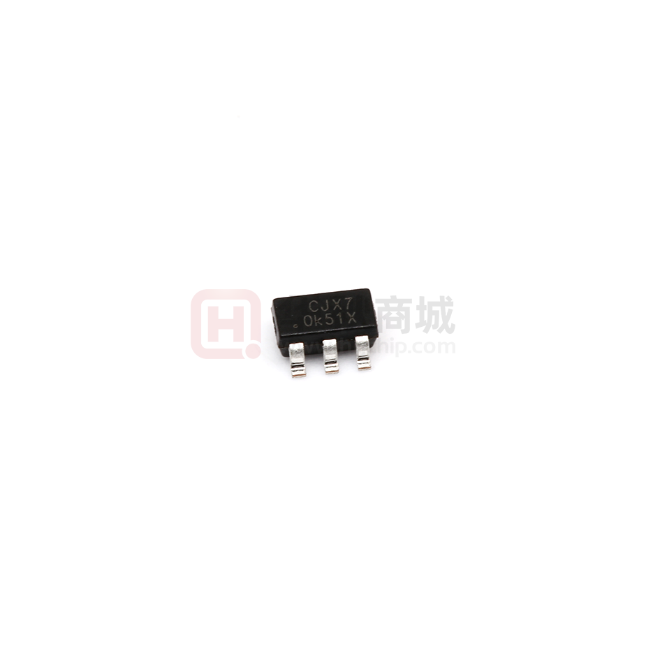
BL9352A is available SOT23-6 Packages.
APPLICATIONS
PIN OUT
www.belling.com.cn
Wide Input Operating Range from 4.5V to 45V
420mΩ internal NMOS
Up to 95% Efficiency at 16V in 12V out L=47uH
with 300mA loading
Internal compensation
Capable of Delivering 600mA continuous output
current
Fixed 1.6MHz PWM operation
Internal soft start
Output voltage adjustable down to 0.795V
Cycle-by-cycle current limit
Current Mode control
Short-circuit protection
Logic Control Shutdown EN can be short to VIN
Thermal shutdown and UVLO
Available in SOT23-6 Package
1
Smart/Industrial/Power Meters
Industrial Applications
Automotive Applications
�BL9352A
PINOUT DESCRIPTION
Pin #
Name
Description
Bootstrap pin for top Switch. In Typ. application, a 0.1uF or larger capacitor should be
1
BST
connected between this pin and the LX pin to supply current to the top Switch gate and top
Switch driver.
2
GND
3
FB
4
EN
Analog Ground
Output feedback pin. In Typ. application, FB senses the output voltage and is regulated by
the control loop to 800mV. Connect a resistive divider at FB.
Drive EN pin high to turn on the regulator and low to turn off the regulator.
Input voltage pin, In Typ. application, VIN supplies power to the IC. Connect a 4.5V to
5
VIN
45V supply to VIN and bypass VIN to GND with a suitably large capacitor to eliminate
noise on the input to the IC.
6
LX
LX is the Switching node that supplies power to the output Connect the output LC filter
from LX to the output load.
TYPICAL APPLICATION
100nF
Vout
4.7uH~47uH
12V/0~600mA
BST
VIN
12.3V ~ 45V
VIN
LX
33pF
10uF
+0.1uF
FB
EN
127K
10uF+0.1uF
+470uF
9.09K
GND
100nF
4.7uH~47uH
BST
VIN
5.3V ~ 45V
VIN
Vout
5V/0~600mA
LX
33pF
10uF
+0.1uF
FB
EN
127K
23.7K
GND
www.belling.com.cn
2
10uF+0.1uF
+470uF
�BL9352A
100nF
Vout
4.7uH~47uH
3.3V/0~600mA
BST
VIN
4.5V ~ 45V
VIN
LX
33pF
FB
EN
10uF
+0.1uF
127K
40.2K
GND
10uF+0.1uF
+470uF
BLOCK DIAGRAM
EN
BST
IN
+
UVLO &
Thermal
shutdown
REG
&REF
Current
Sense
-
+
EA
+
COMP
network
Σ
-
FB
PWM
Logic
DRIVER
OSC
Slope Comp
GND
ABSOLUTE MAXIMUM RATING
Parameter
Input Voltage Range
Max Operating Junction Temperature(Tj)
LX, EN Voltage
BST Voltage
FB Voltage
LX to ground curren
Operating Temperature(To)
SOT23-6
Package Thermal Resistance (jc)
Storage Temperature(Ts)
ESD Rating
Value
-0.3V-50V
150C
–0.3V to VIN+0.3V
–0.3V to LX+6V
–0.3V to 6V
Internally limited
-40C –85C
110C / W
-55C - 150C
2000V
Note: Exceed these limits to damage to the device. Exposure to absolute maximum
rating conditions may affect device reliability.
www.belling.com.cn
3
LX
�BL9352A
ELECTRICAL CHARACTERISTICS
(VIN = VEN = 16V, unless otherwise specified. Typical values are at TA = 25C .)
SYMBOL
VIN
Vin(UVLO)
PARAMETER
Input Voltage Range
Input UVLO
Vin(UVLO)hys
Input UVLO Hysteresis
IQ
Input Supply Current
Isd
VFB
VFB_LOAD
VFB_line
Input Shutdown Current
IFB
Ven_OFF
Ven_OFF
En hys
IEN
Load regulation
Line regulation
Feedback voltage input
current
En high level
En low level
En Hysteresis
Enable input current
Test conditions
MIN
4.5
2.3
Vfb=5V no loading
Ven
很抱歉,暂时无法提供与“BL9352A”相匹配的价格&库存,您可以联系我们找货
免费人工找货- 国内价格
- 1+0.97501
- 10+0.90000
- 30+0.88500