Pb Free Product
BLM2301
P-Channel Enhancement Mode Power MOSFET
DESCRIPTION
D
The BLM2301 uses advanced trench technology to provide
excellent RDS(ON), low gate charge and operation with gate
G
voltages as low as 2.5V. This device is suitable for use as a
load switch or in PWM applications.
S
GENERAL FEATURES
Schematic diagram
● VDS = -20V,ID = -3A
RDS(ON) < 140mΩ @ VGS=-2.5V
RDS(ON) < 110mΩ @ VGS=-4.5V
● High Power and current handing capability
● Lead free product is acquired
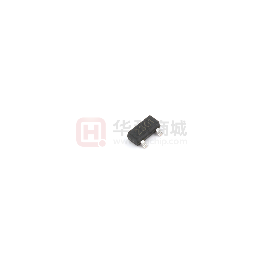
Marking and pin Assignment
● Surface Mount Package
Application
●PWM applications
●Load switch
SOT-23 top view
●Power management
Package Marking And Ordering Information
Device Marking
Device
Device Package
Reel Size
Tape width
Quantity
2301
BLM2301
SOT-23
Ø180mm
8 mm
3000 units
Absolute Maximum Ratings (TA=25℃
℃unless otherwise noted)
Parameter
Symbol
Drain-Source Voltage
VDS
Gate-Source Voltage
VGS
Drain Current-Continuous
ID
Drain Current -Pulsed (Note 1)
IDM
Maximum Power Dissipation
PD
Operating Junction and Storage Temperature Range
TJ,TSTG
Limit
Unit
-20
V
±12
V
-3
A
-10
A
1
W
-55 To 150
℃
125
℃/W
Thermal Characteristic
Thermal Resistance,Junction-to-Ambient (Note 2)
RθJA
Electrical Characteristics (TA=25℃unless otherwise noted)
Parameter
Symbol
Condition
Min
Typ
Max
Unit
Off Characteristics
Drain-Source Breakdown Voltage
BVDSS
VGS=0V ID=-250µA
-20
-24
-
V
Zero Gate Voltage Drain Current
IDSS
VDS=-20V,VGS=0V
-
-
-1
µA
Page1
www.belling.com.cn
V2.0
�Pb Free Product
BLM2301
Gate-Body Leakage Current
IGSS
VGS=±12V,VDS=0V
-
-
±100
nA
Gate Threshold Voltage
VGS(th)
VDS=VGS,ID=-250µA
-0.4
-0.7
-1
V
Drain-Source On-State Resistance
RDS(ON)
VGS=-4.5V, ID=-3A
-
64
110
mΩ
VGS=-2.5V, ID=-2A
-
89
140
mΩ
VDS=-5V,ID=-2.8A
-
9.5
-
S
-
405
-
PF
-
75
-
PF
On Characteristics (Note 3)
Forward Transconductance
gFS
Dynamic Characteristics (Note4)
Input Capacitance
Clss
Output Capacitance
Coss
Reverse Transfer Capacitance
Crss
-
55
-
PF
Turn-on Delay Time
td(on)
-
11
-
nS
Turn-on Rise Time
tr
VDD=-10V,ID=-1A
-
35
-
nS
td(off)
VGS=-4.5V,RGEN=10Ω
-
30
-
nS
-
10
-
nS
-
3.3
12
nC
-
0.7
-
nC
-
1.3
-
nC
-
-
-1.2
V
-
-
-1.3
A
VDS=-10V,VGS=0V,
F=1.0MHz
Switching Characteristics (Note 4)
Turn-Off Delay Time
Turn-Off Fall Time
tf
Total Gate Charge
Qg
Gate-Source Charge
Qgs
Gate-Drain Charge
Qgd
VDS=-10V,ID=-3A,
VGS=-2.5V
Drain-Source Diode Characteristics
Diode Forward Voltage (Note 3)
VSD
Diode Forward Current (Note 2)
IS
VGS=0V,IS=1.3A
Notes:
1. Repetitive Rating: Pulse width limited by maximum junction temperature.
2. Surface Mounted on FR4 Board, t ≤ 10 sec.
3. Pulse Test: Pulse Width ≤ 300µs, Duty Cycle ≤ 2%.
4. Guaranteed by design, not subject to production
Page2
www.belling.com.cn
V2.0
�Pb Free Product
BLM2301
TYPICAL ELECTRICAL AND THERMAL CHARACTERISTICS
ton
tr
td(on)
toff
tf
td(off)
90%
VOUT
90%
INVERTED
10%
10%
90%
VIN
50%
50%
10%
PULSE WIDTH
Figure 2:Switching Waveforms
PD Power(W)
ID- Drain Current (A)
Figure 1:Switching Test Circuit
TJ-Junction Temperature(℃)
TJ-Junction Temperature(℃)
Figure 4 Drain Current
ID- Drain Current (A)
Rdson On-Resistance(Ω)
Figure 3 Power Dissipation
Vds Drain-Source Voltage (V)
ID- Drain Current (A)
Figure 5 Output CHARACTERISTICS
Page3
Figure 6 Drain-Source On-Resistance
www.belling.com.cn
V2.0
�Pb Free Product
ID- Drain Current (A)
Normalized On-Resistance
BLM2301
Vgs Gate-Source Voltage (V)
TJ-Junction Temperature(℃)
Figure 8 Drain-Source On-Resistance
C Capacitance (pF)
Rdson On-Resistance(Ω)
Figure 7 Transfer Characteristics
Vgs Gate-Source Voltage (V)
Vds Drain-Source Voltage (V)
Figure 10 Capacitance vs Vds
Vgs Gate-Source Voltage (V)
Is- Reverse Drain Current (A)
Figure 9 Rdson vs Vgs
Qg Gate Charge (nC)
Figure 11 Gate Charge
Page4
Vsd Source-Drain Voltage (V)
Figure 12 Source- Drain Diode Forward
www.belling.com.cn
V2.0
�Pb Free Product
ID- Drain Current (A)
BLM2301
Vds Drain-Source Voltage (V)
Safe Operation Area
r(t),Normalized Effective
Transient Thermal Impedance
Figure 13
Square Wave Pluse Duration(sec)
Figure 14 Normalized Maximum Transient Thermal Impedance
Page5
www.belling.com.cn
V2.0
�Pb Free Product
BLM2301
SOT-23 PACKAGE INFORMATION
Dimensions in Millimeters (UNIT:mm)
Symbol
A
A1
A2
b
c
D
E
E1
e
e1
L
L1
θ
Dimensions in Millimeters
MIN.
MAX.
0.900
1.150
0.000
0.100
0.900
1.050
0.300
0.500
0.080
0.150
2.800
3.000
1.200
1.400
2.250
2.550
0.950TYP
1.800
2.000
0.550REF
0.300
0.500
0°
8°
NOTES
1. All dimensions are in millimeters.
2. Tolerance ±0.10mm (4 mil) unless otherwise specified
3. Package body sizes exclude mold flash and gate burrs. Mold flash at the non-lead sides should be less than 5 mils.
4. Dimension L is measured in gauge plane.
5. Controlling dimension is millimeter, converted inch dimensions are not necessarily exact.
Page6
www.belling.com.cn
V2.0
�
很抱歉,暂时无法提供与“BLM2301”相匹配的价格&库存,您可以联系我们找货
免费人工找货- 国内价格
- 1+0.27440
- 200+0.17696
- 1500+0.15456
- 3000+0.13664
- 国内价格
- 20+0.28793
- 200+0.23544
- 600+0.20628
- 国内价格
- 5+0.16701
- 20+0.15201
- 100+0.13701
- 500+0.12201
- 1000+0.11501
- 2000+0.11001