Pb Free Product
BLM8205
N-Channel Enhancement Mode Power MOSFET
Description
D1
D2
The BLM8205 uses advanced trench technology to provide
G1
excellent RDS(ON), low gate charge and operation with gate
G2
voltages as low as 2.5V. This device is suitable for use as a
Battery protection or in other Switching application.
S1
S2
Schematic diagram
General Features
● VDS = 19.5V,ID = 4A
Typ.RDS(ON) = 21mΩ @ VGS=4.5V
Typ.RDS(ON) = 27mΩ @ VGS=2.5V
● High Power and current handing capability
● Lead free product is acquired
Marking and pin Assignment
● Surface Mount Package
Application
●Battery protection
●Load switch
●Power management
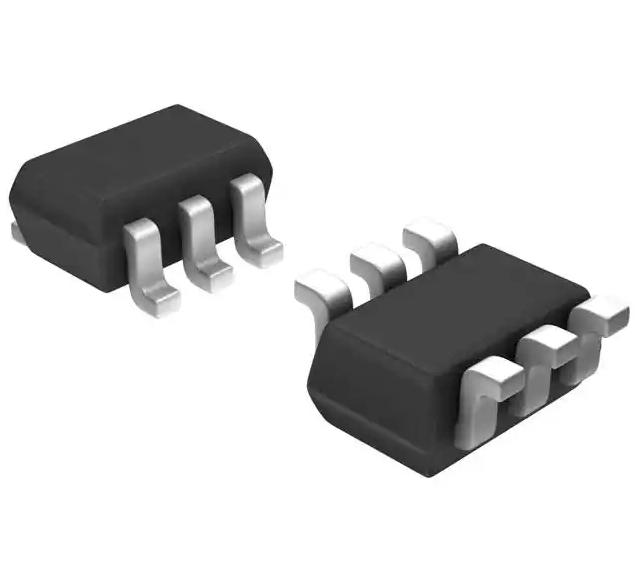
SOT23-6L top view
Package Marking And Ordering Information
Device Marking
Device
Device Package
Reel Size
Tape width
Quantity
8205
BLM8205
SOT23-6L
Ø180mm
8mm
3000 units
Absolute Maximum Ratings (TA=25℃unless otherwise noted)
Parameter
Symbol
Drain-Source Voltage
VDS
Gate-Source Voltage
VGS
Drain Current-Continuous
ID
Drain Current-Pulsed (Note 1)
IDM
Maximum Power Dissipation
PD
Operating Junction and Storage Temperature Range
TJ,TSTG
Limit
Unit
19.5
V
±8
V
4
A
25
A
1.25
W
-55 To 150
℃
100
℃/W
Thermal Characteristic
Thermal Resistance,Junction-to-Ambient (Note 2)
RθJA
Electrical Characteristics (TA=25℃unless otherwise noted)
Parameter
Symbol
Condition
Min
Typ
Max
Unit
Off Characteristics
Drain-Source Breakdown Voltage
BVDSS
VGS=0V ID=250µA
19.5
21
-
V
Zero Gate Voltage Drain Current
IDSS
VDS=19.5V,VGS=0V
-
-
1
µA
Page1
www.belling.com.cn
V2.2
�Pb Free Product
BLM8205
Gate-Body Leakage Current
IGSS
VGS=±8V,VDS=0V
-
-
±100
nA
Gate Threshold Voltage
VGS(th)
VDS=VGS,ID=250µA
0.45
0.7
1.2
V
Drain-Source On-State Resistance
RDS(ON)
VGS=4.5V, ID=4A
-
21
27
mΩ
VGS=2.5V, ID=3A
-
27
40
mΩ
VDS=5V,ID=4A
-
10
-
S
-
800
-
PF
-
155
-
PF
On Characteristics (Note 3)
Forward Transconductance
gFS
Dynamic Characteristics (Note4)
Input Capacitance
Clss
Output Capacitance
Coss
Reverse Transfer Capacitance
Crss
-
125
-
PF
Turn-on Delay Time
td(on)
-
18
-
nS
Turn-on Rise Time
tr
VDD=10V,ID=1A
-
5
-
nS
td(off)
VGS=4V,RGEN=10Ω
-
43
-
nS
-
20
-
nS
-
11
-
nC
-
2.3
-
nC
-
2.5
-
nC
1.3
V
2
A
VDS=8V,VGS=0V,
F=1.0MHz
Switching Characteristics (Note 4)
Turn-Off Delay Time
Turn-Off Fall Time
tf
Total Gate Charge
Qg
Gate-Source Charge
Qgs
Gate-Drain Charge
Qgd
VDS=10V,ID=4A,
VGS=4.5V
Drain-Source Diode Characteristics
Diode Forward Voltage (Note 3)
VSD
Diode Forward Current (Note 2)
IS
VGS=0V,IS=2A
-
-
Notes:
1. Repetitive Rating: Pulse width limited by maximum junction temperature.
2. Surface Mounted on FR4 Board, t ≤ 10 sec.
3. Pulse Test: Pulse Width ≤ 300µs, Duty Cycle ≤ 2%.
4. Guaranteed by design, not subject to production
Page2
www.belling.com.cn
V2.2
�Pb Free Product
BLM8205
TYPICAL ELECTRICAL AND THERMAL CHARACTERISTICS
Vdd
Rgen
D
tr
td(on)
Rl
Vin
Vgs
ton
td(off)
90%
Vout
VOUT
G
toff
tf
90%
INVERTED
10%
10%
90%
S
VIN
50%
50%
10%
PULSE WIDTH
Figure 2:Switching Waveforms
PD Power(W)
ID- Drain Current (A)
Figure 1:Switching Test Circuit
TJ-Junction Temperature(℃)
TJ-Junction Temperature(℃)
Figure 4 Drain Current
ID- Drain Current (A)
Rdson On-Resistance(mΩ)
Figure 3 Power Dissipation
Vds Drain-Source Voltage (V)
ID- Drain Current (A)
Figure 5 Output CHARACTERISTICS
Page3
Figure 6 Drain-Source On-Resistance
www.belling.com.cn
V2.2
�Pb Free Product
ID- Drain Current (A)
Normalized On-Resistance
BLM8205
TJ-Junction Temperature(℃)
Vgs Gate-Source Voltage (V)
Figure 8 Drain-Source On-Resistance
C Capacitance (pF)
Rdson On-Resistance(mΩ)
Figure 7 Transfer Characteristics
Vds Drain-Source Voltage (V)
Vgs Gate-Source Voltage (V)
Figure 10 Capacitance vs Vds
Vgs Gate-Source Voltage (V)
Is- Reverse Drain Current (A)
Figure 9 Rdson vs Vgs
Qg Gate Charge (nC)
Figure 11 Gate Charge
Page4
Vsd Source-Drain Voltage (V)
Figure 12 Source- Drain Diode Forward
www.belling.com.cn
V2.2
�Pb Free Product
ID- Drain Current (A)
BLM8205
Vds Drain-Source Voltage (V)
Safe Operation Area
Transient Thermal Impedance
r(t),Normalized Effective
Figure 13
Square Wave Pluse Duration(sec)
Figure 14 Normalized Maximum Transient Thermal Impedance
Page5
www.belling.com.cn
V2.2
�Pb Free Product
BLM8205
SOT23-6L PACKAGE INFORMATION
Page6
www.belling.com.cn
V2.2
�