BUT11
NPN SILICON POWER TRANSISTOR
Rugged Triple-Diffused Planar Construction
100 W at 25°C Case Temperature
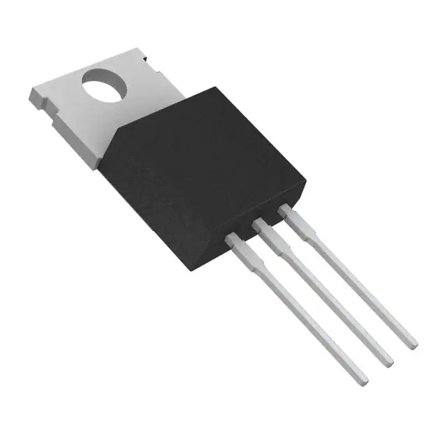
TO-220 PACKAGE
(TOP VIEW)
5 A Continuous Collector Current
This series isOBSOLETEAND
not recommended for new designs.
B
1
C
2
E
3
Pin 2 is in electrical contact with the mounting base.
MDTRACA
absolute maximum ratings at 25°C case temperature (unless otherwise noted)
RATING
Collector-base voltage (IE = 0)
Collector-emitter voltage (VBE = 0)
Collector-emitter voltage (IB = 0)
Emitter-base voltage
Continuous collector current
SYMBOL
VALUE
UNIT
VCBO
850
V
VCES
E
T
E
L
O
S
B
O
Peak collector current (see Note 1)
V CEO
VEBO
IC
ICM
Continuous device dissipation at (or below) 25°C case temperature
Ptot
Storage temperature range
Tstg
Operating junction temperature range
NOTE
Tj
850
400
V
V
10
V
10
A
5
100
-65 to +150
-65 to +150
A
W
°C
°C
1: This value applies for tp ≤ 10 ms, duty cycle ≤ 2%.
MAY 1989 - REVISED SEPTEMBER 2002
Specifications are subject to change without notice.
1
�BUT11
NPN SILICON POWER TRANSISTOR
electrical characteristics at 25°C case temperature (unless otherwise noted)
PARAMETER
VCEO(sus)
ICES
IEBO
hFE
V CE(sat)
VBE(sat)
ft
Cob
Collector-emitter
sustaining voltage
TEST CONDITIONS
IC =
0.1 A
L = 25 mH
Collector-emitter
VCE = 850 V
VBE = 0
cut-off current
VCE = 850 V
VBE = 0
VEB =
10 V
IC = 0
VCE =
5V
Emitter cut-off
current
Forward current
transfer ratio
Collector-emitter
saturation voltage
Base-emitter
saturation voltage
Current gain
bandwidth product
Output capacitance
MIN
(see Note 2)
TYP
MAX
400
V
50
TC = 125°C
500
1
IC = 0.5 A
(see Notes 3 and 4)
UNIT
20
µA
mA
60
IB =
0.6 A
IC =
3A
(see Notes 3 and 4)
1.5
V
IB =
0.6 A
IC =
3A
(see Notes 3 and 4)
1.3
V
VCE =
10 V
IC = 0.5 A
f=
1 MHz
12
MHz
VCB =
20 V
IE = 0
f = 0.1 MHz
110
pF
NOTES: 2. Inductive loop switching measurement.
3. These parameters must be measured using pulse techniques, tp = 300 µs, duty cycle ≤ 2%.
4. These parameters must be measured using voltage-sensing contacts, separate from the current carrying contacts.
thermal characteristics
E
T
E
L
O
S
B
O
PARAMETER
RθJC
MIN
TYP
Junction to case thermal resistance
MAX
UNIT
1.25
°C/W
inductive-load-switching characteristics at 25°C case temperature (unless otherwise noted)
PARAMETER
†
tsv
Voltage storage time
tfi
Current fall time
tsv
Voltage storage time
tfi
Current fall time
TEST CONDITIONS
†
IC = 3 A
IB(on) = 0.6A
VCC = 50 V
(see Figures 1 and 2)
IC = 3 A
IB(on) = 0.6A
VCC = 50 V
TC = 100°C
MIN
VBE(off) = -5 V
VBE(off) = -5 V
MAX
UNIT
1.4
µs
150
ns
1.5
µs
300
ns
Voltage and current values shown are nominal; exact values vary slightly with transistor parameters.
������
2
TYP
�
�������
MAY 1989 - REVISED SEPTEMBER 2002
Specifications are subject to change without notice.
�BUT11
NPN SILICON POWER TRANSISTOR
PARAMETER MEASUREMENT INFORMATION
33 Ω
+5V
D45H11
BY205-400
33 Ω
BY205-400
RB
(on)
1 pF
180 µH
V Gen
1 kΩ
68 Ω
0.02 µF
vcc
2N2222
BY205-400
Vclamp = 400 V
TUT
1 kΩ
+5V
270 Ω
E
T
E
L
O
S
B
O
BY205-400
5X BY205-400
1 kΩ
2N2904
Adjust pw to obtain IC
D44H11
47 Ω
For IC < 6 A
VCC = 50 V
For IC ≥ 6 A
VCC = 100 V
V
100 Ω
BE(off)
Figure 1. Inductive-Load Switching Test Circuit
I B(on)
A - B = tsv
B - C = trv
D - E = tfi
E - F = tti
A (90%)
IB
Base Current
C
B - E = txo
V
CE
B
90%
10%
Collector Voltage
D (90%)
E (10%)
I
C(on)
Collector Current
F (2%)
NOTES: A. Waveforms are monitored on an oscilloscope with the following characteristics: t r < 15 ns, Rin > 10 Ω, C in < 11.5 pF.
B. Resistors must be noninductive types.
Figure 2. Inductive-Load Switching Waveforms
������
�
�������
MAY 1989 - REVISED SEPTEMBER 2002
Specifications are subject to change without notice.
3
�BUT11
NPN SILICON POWER TRANSISTOR
MAXIMUM SAFE OPERATING REGIONS
MAXIMUM FORWARD-BIAS
SAFE OPERATING AREA
IC - Collector Current - A
100
SAP791AB
10
1·0
0.1
tp =
10 µs
tp = 100 µs
1 ms
tp =
tp = 10 ms
DC Operation
E
T
E
L
O
S
B
O
0·01
1·0
10
100
1000
VCE - Collector-Emitter Voltage - V
Figure 3.
������
4
�
�������
MAY 1989 - REVISED SEPTEMBER 2002
Specifications are subject to change without notice.
�
很抱歉,暂时无法提供与“BUT11-S”相匹配的价格&库存,您可以联系我们找货
免费人工找货