PL
IA
NT
Features
CO
M
■ Concave terminals
*R
oH
S
■ RoHS compliant*
■ 8 bit multiple applications
■ Smallest bussed chip array
■ E 24 Series from 10 ohms to 1 megohm
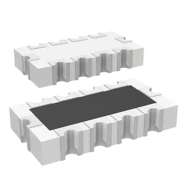
CAT25 - Thick Film Chip Resistor Arrays
How To Order
Electrical Characteristics
Parameters
Number of Resistors
Resistance Range E24
Resistance Tolerance
Power Rating/Resistor
Rating Temperature
T.C.R.
Maximum Operating Voltage
Operating Temperature
CAT25
8
10 ohms to 1 megohm
5%
62.5 mW
+70 °C
±200 ppm/°C
25 V
-55 °C to +125 °C
Test Method
JIS-C-5202.5.1
Characteristics
±(3 % +0.1 ohm)
±(5 % +0.1 ohm)
±(3 % +0.1 ohm)
±(1 % +0.1 ohm)
±(1 % +0.1 ohm)
±(2 % +0.1 ohm)
±(1 % +0.1 ohm)
1000 megohms minimum
50 VRMS
>95 %
Outline Drawing
Pin Style
T = Concave
Model
JIS-C-5202.5.2
Resistance Value
103 = 10K ohms
Tolerance
J=5%
Electrical Circuit
A = 8 Resistors, Bussed Type
Environmental Characteristics
Specification
Short Time Overload
Load Life
Humidity Load Life
Resistance to Soldering Heat
Terminal Strength
Temperature Cycle
Vibration
Insulation Resistance
Dielectric Withstanding Voltage
Lead Solderability
CA T 25 - 103 J A LF
Product
CA = Chip Array
Test Method
JIS-C-5202.5.5
JIS-C-5202.7.10
JIS-C-5202.7.9
JIS-C-5202.6.4
JIS-C-5202.6.
JIS-C-5202.7.4
JIS-C-5202.6.3
JIS-C-5202.5.6
JIS-C-5202.5.7
JIS-C-5202.6.5
Terminations
LF = Tin-plated (RoHS compliant)
For Standard Values Used in
Capacitors, Inductors, and Resistors,
click here.
Land Pattern
4.8 - 5.2
(.190 - .205)
2.10 ± 0.20
(.083 ± .008)
2.8 - 3.0
(.110 - .118)
0.25 ± 0.20
(.010 ± .008)
0.30 ± 0.20
(.012 ± .008)
4.00 ± 0.20
(.157 ± .008)
DIMENSIONS:
0.35 ± 0.20
(.014 ± .008)
0.50 ± 0.20
(.020 ± .008)
3.2 - 3.5
(.125 - .138)
3.3 - 3.4
(.130 - .133)
0.55 ± 0.10
(.022 ± .004)
0.80 ± 0.10
(.032 ± .004)
0.9 - 1.1
(.035 - .043)
MM
(INCHES)
0.4 - 0.5
(.016 - .020)
0.80
(.032)
Electrical Circuit
DIA.
0.30 +0.10/-0.20
(.012 +.004/-.008)
0.40 ± 0.20
(.016 ± .008)
WARNING
Cancer and Reproductive Harm
www.P65Warnings.ca.gov
*RoHS Directive 2015/863, Mar 31, 2015 and Annex.
Specifications are subject to change without notice. Users should verify actual device performance in their specific
applications. The products described herein and this document are subject to specific legal disclaimers as set forth on the
last page of this document, and at www.bourns.com/docs/legal/disclaimer.pdf.
�CAT25 - Thick Film Chip Resistor Arrays
Soldering Profile for RoHS Compliant Chip Resistors and Arrays
275
Maximum of 20 seconds between
260 °C peak
+255 °C and +260 °C
255 °C
225
Temperature (°C)
220 °C
190 °C
60 - 90
seconds
175
Ramp Down
6 °C/second
150 °C
125
60 - 120 seconds
10 seconds minimum
75
Ramp Up
3 °C/second maximum
25
0
50
100
Packaging
Material
12
(.472) embossed tape
4,000 pcs. per reel
Substrate
150
Time (seconds)
200
250
300
Alumina 96
Element
Ruthenium Oxide
Coating
Glass
Terminal
Plated Ni+Sn
Asia-Pacific: Tel: +886-2 2562-4117 • Email: asiacus@bourns.com
EMEA: Tel: +36 88 885 877 • Email: eurocus@bourns.com
The Americas: Tel: +1-951 781-5500 • Email: americus@bourns.com
www.bourns.com
REV. 09/19
Specifications are subject to change without notice.
Users should verify actual device performance in their specific applications.
The products described herein and this document are subject to specific legal disclaimers as set forth on the last page of this document, and at www.bourns.com/docs/legal/disclaimer.pdf.
�Legal Disclaimer Notice
This legal disclaimer applies to purchasers and users of Bourns® products manufactured by or on behalf of Bourns, Inc. and
P[Z�HɉSPH[LZ��JVSSLJ[P]LS`��¸)V\YUZ¹��
Unless otherwise expressly indicated in writing, Bourns® products and data sheets relating thereto are subject to change
^P[OV\[�UV[PJL���
很抱歉,暂时无法提供与“CAT25-560JALF”相匹配的价格&库存,您可以联系我们找货
免费人工找货