PL
IA
Features
■ ■ ■ ■
Applications
■ ■ ■ ■
NT
Lead free device (RoHS compliant*) Low profile Low power loss, high efficiency UL 94V-0 classification
High frequency switching power supplies Inverters Free wheeling Polarity protection
*R
oH
S
CO
M
CD1408-R1200~R11000 – Surface Mount Rectifier Diode
General Information
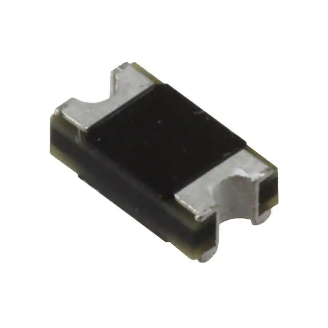
The markets of portable communications, computing and video equipment are challenging the semiconductor industry to develop increasingly smaller electronic components. Bourns offers Rectifier Diodes for rectification applications, in compact chip package 1408 size format (compatible with SOD87, SOD123 formats), which offers PCB real estate savings and are considerably smaller than most competitive parts. The Glass Passivated Rectifier Diodes offer a forward current of 1 A with a choice of repetitive peak reverse voltage of 200 V up to 1000 V. Bourns Chip Diodes conform to JEDEC standards, are easy to handle on standard pick and place equipment and their flat configuration minimizes roll away.
®
Tin Plated Connectors
FRP Substrate and Epoxy Underfill
Electrical Characteristics (@ TA = 25 °C Unless Otherwise Noted) Parameter Symbol CD1408R1200 R1400 R1600 R1800 R11000 Unit
Maximum Repetitive Peak Reverse Voltage Maximum RMS Voltage Maximum DC Blocking Voltage Max. Average Forward Rectified Current
1
VRRM VRMS VDC I(AV) IR IR IR CJ VF Trr IFSM
200 140 200
400 280 400
600 420 600 1.0 1.0 30.0 50.0 12 1.0 3000 30.0
800 560 800
1000 700 1000
V V V A µA µA µA pF V ns A
DC Reverse Current @ Rated DC Blocking Voltage (@Ta = 25 °C) DC Reverse Current @ Rated DC Blocking Voltage (@Ta = 125 °C) DC Reverse Current @ Rated DC Blocking Voltage (@Ta = 150 °C) Typical Junction Capacitance2 Instantaneous Forward Voltage @ IF = 1 A Maximum Reverse Recovery Time
3
Peak forward surge current 8.3 ms single half sine-wave superimposed on rated load (JEDEC Method)
Notes: 1 See Forward Derating Curve. 2 Measured @ 1.0 MHz and applied reverse voltage of 4.0 VDC. 3 Reverse recovery test condition: IF = 0.5 A, IR = 1.0 A, Irr = 0.25 A
Thermal Characteristics (@ TA = 25 °C Unless Otherwise Noted) Parameter Operating Temperature Range Storage Temperature Range Symbol TJ TSTG CD1408-R1200~R11000 -65 to +175 -65 to +175 Unit °C °C
*RoHS Directive 2002/95/EC Jan 27 2003 including Annex. Specifications are subject to change without notice. Customers should verify actual device performance in their specific applications.
�CD1408-R1200~R11000 – Surface Mount Rectifier Diode
Product Dimensions This is a lead free product, packaged with FRP substrate and is epoxy underfilled. The terminals are pure tin plated and are solderable per MIL-STD-750, Method 2026. The package weighs approximately 0.02 g. The package and dimensions are shown below.
3.2 - 3.60 (0.126 - 0.142)
Recommended Footprint The device will mount onto existing JEDEC SOD-87 footprint.
How To Order
CD 1408 - R 1 400
Common Code CD = Chip Diode Package 1408 = ~0.14 x 0.08 ˝ Function R = Rectifier Forward Current I(AV) 1=1A Reverse Voltage 200 = 200 V 400 = 400 V 600 = 600 V 800 = 800 V 1000 = 1000 V
1.70 - 2.10 (0.067 - 0.083)
B R1D
0.40 R (0.016)
0.50 - 0.90 (0.020 - 0.035)
0.50 - 0.90 (0.020 - 0.035)
Typical Part Marking CD1408-R1200 .......................................................................... CD1408-R1400 .......................................................................... CD1408-R1600 .......................................................................... CD1408-R1800 .......................................................................... CD1408-R11000 ........................................................................ R1D R1G R1J R1K R1M
0.95 - 1.35 (0.037 - 0.053)
DIMENSIONS:
MM (INCHES)
Specifications are subject to change without notice. Customers should verify actual device performance in their specific applications.
�CD1408-R1200~R11000 – Surface Mount Rectifier Diode
Packaging Information
The product will be dispensed in Tape and Reel format (see diagram below).
P 0 P 1
d
E Index Hole
T
120 ° F W B D2 D1 D
P Trailer
A Device
C Leader
End
....... .......
10 pitches (min.)
....... .......
....... .......
....... .......
10 pitches (min.)
W1 Start DIMENSIONS: MM (INCHES)
Direction of Feed
Devices are packed in accordance with EIA standard RS-481-A and specifications shown here.
Item Carrier Width Carrier Length Carrier Depth Sprocket Hole Reel Outside Diameter Reel Inner Diameter Feed Hole Diameter Sprocket Hole Position Punch Hole Position Punch Hole Pitch Sprocket Hole Pitch Embossment Center Overall Tape Thickness Tape Width Reel Width Quantity per Reel
Symbol A B C d D D1 D2 E F P P0 P1 T W W1 —
1408
1.90 ±0.10 (0.075 - 0.004) 4.30 ±0.10 (0.169 - 0.004) 1.80 ±0.10 (0.071 - 0.004) 1.55 ±0.05 (0.061 - 0.002) 178 (7.008) 80.0 Min. (3.150) 13.0 ±0.20 (0.512 - 0.008) 1.75 ±0.10 (0.069 - 0.004) 3.50 ±0.05 (0.138 - 0.002) 4.00 ±0.10 (0.157 - 0.004) 4.00 ±0.10 (0.157 - 0.004) 2.00 ±0.05 (0.079 - 0.002) 0.20 ±0.10 (0.008 - 0.004) 8.00 ±0.20 (0.315 - 0.008) 13.5 Max. (0.531)
2,500
Specifications are subject to change without notice. Customers should verify actual device performance in their specific applications.
�CD1408-R1200~R11000 – Surface Mount Rectifier Diode
Performance Graphs Forward Current Derating Curve
1.50 1.25 1.00 0.75 0.50 0.25 0 0 50 75 100 125 150 175 200 Lead Temperature (°C) 60 Hz Resistive or Inductive Load Peak Forward Surge Current (Amps) Average Forward Current (Amps)
Maximum Non-Repetitive Surge Current
30 25 20 15 10 0 1 10 Number of Cycles at 60 Hz 100 Pulse Width 8.3 ms Single Half Sine-Wave (JEDEC Method)
Typical Forward Characteristics
10.00
Typical Reverse Characteristics
100
1.00
Instantaneous Reverse Leakage Current (µA)
Instantaneous Forward Current (Amps)
10
TJ = 125 °C
0.10
1
TJ = 100 °C
Pulse Width = 300 µs 1 % Duty Cycle 0.01 0.4 0.6 0.8 1.0 1.2 1.4 1.6 Instantaneous Forward Voltage (Volts)
0.1 0 20 40 60 80 100 110 Percent of Rated Peak Reverse Voltage (%)
Typical Junction Capacitance
200 100 60 40 Junction Capacitance (pF)
Reliable Electronic Solutions
20 10 6 4 TJ = 25 °C 2 1 0.1 0.2 0.4 1.0 2 4 10 20 40 100 Reverse Voltage (Volts)
Asia-Pacific: Tel: +886-2 2562-4117 • Fax: +886-2 2562-4116 Europe: Tel: +41-41 768 5555 • Fax: +41-41 768 5510 The Americas: Tel: +1-951 781-5500 • Fax: +1-951 781-5700 www.bourns.com
REV. 05/06
Specifications are subject to change without notice. Customers should verify actual device performance in their specific applications.
�
很抱歉,暂时无法提供与“CD1408-R11000”相匹配的价格&库存,您可以联系我们找货
免费人工找货- 国内价格 香港价格
- 3000+0.698923000+0.09046
- 6000+0.631416000+0.08172
- 9000+0.596999000+0.07727
- 15000+0.5582715000+0.07226
- 21000+0.5353521000+0.06929
- 30000+0.5130530000+0.06640