CO
LO & MP
LI
GE
AN
N
T
FR
EE
*R
oH
S
**
HA
Features
Applications
■ RoHS compliant*
■ Ethernet - 10/100/1000 Base T
■ Halogen free**
■ Firewire and USB
■ ESD protection >15 kV
■ Portable electronics
■ Protects Vcc and two data lines
■ Video/graphic cards
CD143A-SR05LC - Steering/TVS Diode Array Series
General Information
Additional Information
®
The Bourns Model CD143A-SR05LC device provides
ESD, EFT and surge protection for the external ports of
portable electronic devices such as cellphones, handheld
electronics and personal computers.
The ESD protection provided by the component enables a
data port to withstand a minimum ±8 KV Contact / ±15 KV
Air Discharge per the ESD test method specified in IEC
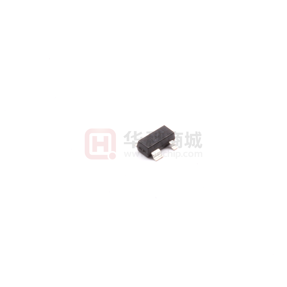
61000-4-2. The device measures 2.80 mm x 1.20 mm and
is available in a SOT-143 package intended to be mounted
directly onto an FR4 printed circuit board.The Bourns®
device will meet IEC 61000-4-2 (ESD), IEC 61000-4-4
(EFT) and IEC 61000-4-5 (Surge) requirements.
Click these links for more information:
4
GND
REF
1
PRODUCT TECHNICAL INVENTORY SAMPLES
SELECTOR LIBRARY
I/O
2
3
CONTACT
I/O
Absolute Maximum Ratings (@ TA = 25 °C Unless Otherwise Noted)
Parameter
Symbol
Value
Unit
Peak Pulse Current (tp= 8/20 μs)
IPP
13
A
Operating Temperature
TJ
-55 to +125
°C
TSTG
-55 to +150
°C
Vf
1
V
Storage Temperature
Forward Voltage (If= 15 mA, Pin 1-4)
Electrical and Thermal Characteristics (@ TA = 25 °C Unless Otherwise Noted)
Parameter
Symbol
Value
Unit
Breakdown Voltage Minimum @ 2 mA 1
VBR
6.1
V
Working Peak Voltage 1
VWM
5.0
V
Clamping Voltage Maximum @ IP = 5 A 2,4
Clamping Voltage Maximum @ IPP 2,4
Leakage Current @ VWM 1
Capacitance Maximum between I/O Pins and Ground
@ VR = 0 V, f = 1 MHz 3
VC
9.0
V
VC
12.5 @ 13 A
V
ID
1.0
μA
CIN
3
pF
Notes:
1. From Pin 4 to Pin 1.
2. See Pulse Wave Form.
3. Pin 1 (GND) connected to Ground, Pin 4 (REF) connected to 5 V.
4. I/O to GND, REF connected to 5 V and GND connected to Ground.
WARNING Cancer and Reproductive Harm - www.P65Warnings.ca.gov
* RoHS Directive 2015/863, Mar 31, 2015 and Annex.
** Bourns considers a product to be “halogen free” if (a) the Bromine (Br) content is 900 ppm or less; (b) the Chlorine (Cl) content is 900 ppm or less; and (c) the total Bromine (Br)
and Chlorine (Cl) content is 1500 ppm or less.
Specifications are subject to change without notice.
Users should verify actual device performance in their specific applications.
The products described herein and this document are subject to specific legal disclaimers as set forth on the last page of this document, and at www.bourns.com/docs/legal/disclaimer.pdf.
�CD143A-SR05LC - Steering/TVS Diode Array Series
Product Dimensions
This is a molded JEDEC SOT-143 device. It has a flammability rating of UL 94V-0.
The dimensions for the packaged device are shown below.
Dimensions
A
B
D
G
C
A
2.80 - 3.04
(0.110 - 0.12)
B
1.78 - 2.03
(0.070 - 0.080)
C
2.11 - 2.55
(0.083 - 0.100)
D
1.2 - 1.4
(0.047 - 0.055)
E
0.35 - 0.5
(0.014 - 0.020)
F
0.76 - 0.93
(0.030 - 0.037)
G
0.08 - 0.18
(0.003 - 0.007)
H
0.46 - 0.60
(0.018 - 0.024)
I
0.84 - 1.14
(0.033 - 0.045)
J
0.72 - 0.83
(0.028 - 0.033)
K
0.013 - 0.10
(0.0005 - 0.004)
H
F
E
DIMENSIONS:
I
J
MM
(INCHES)
K
Recommended Pad Layout
Block Diagram
This is the footprint recommended for this SOT-143 device.
2.92
(0.115)
The device block diagram below includes the pin names and basic
electrical connections associated with each channel.
1.92
(0.076)
GND
1
I/O
2
4
REF
3
I/O
1.4
(0.055)
3.6
(0.142)
2.2
(0.087)
0.8
(0.031)
1.72
(0.068)
1.4
(0.055)
Typical Part Marking
1.4
(0.055)
1.00
(0.039)
CD143A-SR05LC .........................................................................5LC
0.52
(0.020)
DIMENSIONS:
MM
(INCHES)
Specifications are subject to change without notice.
Users should verify actual device performance in their specific applications.
The products described herein and this document are subject to specific legal disclaimers as set forth on the last page of this document, and at www.bourns.com/docs/legal/disclaimer.pdf.
�CD143A-SR05LC - Steering/TVS Diode Array Series
Performance Graphs
15
14
13
12
11
10
9
8
7
6
5
4
3
2
1
0
Pulse Wave Form
IPP – Peak Pulse Current (% of IPP)
Clamping Voltage (V)
Typical Clamping Voltage vs. Peak Pulse Current
Waveform
Parameters:
tr=8 µs
td=20 µs
I/O pin to GND pin
120
Test Waveform Parameters
tt = 8 µs
td = 20 µs
tt
100
80
et
60
40
td = t|IPP/2
20
0
5
0
10
15
20
25
30
t – Time (µs)
4
5
6
7
8
9
10
11
12
13
Peak Pulse Current (A)
Typical Capacitance vs. Reverse Voltage
Power Derating Curve
4.0
100
% of Rated Power
Input Capacitance (pF)
3.5
3.0
2.5
2.0
60
40
20
1.5
1.0
0
VDD = 5 V, GND = 0 V, f = 1 MHz, T = 25 ° C
0.5
0.0
80
0
25
50
75
100
125
150
TL – Lead Temperature (°C)
0
1
2
3
4
5
Input Voltage (V)
How to Order
CD 143A - SR 05 LC
Common Code
Chip Diode
Package
143A = SOT-143
Model
SR = Steering Diode Array
Workint Peak Voltage
05 = 5.0 VWM (Volts)
Capacitance
LC = Low Capacitance
Specifications are subject to change without notice.
Users should verify actual device performance in their specific applications.
The products described herein and this document are subject to specific legal disclaimers as set forth on the last page of this document, and at www.bourns.com/docs/legal/disclaimer.pdf.
�CD143A-SR05LC - Steering/TVS Diode Array Series
Application Information
The Model CD143A-SR05LC is designed to protect two data lines
against transient overvoltage events, as well as to limit the transient
voltage on the 5 V supply line of the protected device.
To optimize the performance of the protection design, connections
to the CD143A-SR05LC should be as short as possible. This will
minimize the parasitic inductance of the printed circuit board traces.
An optional 0.1 μF bypass chip capacitor can be added from Pin 4
to Ground to enhance the ESD performance of the design when the
nearest bypass capacitor is a significant distance from the Model
CD143A-SR05LC.
Pin 1 must be connected to the local Ground used by the protected
device and Pin 4 must be connected to the 5 V supply rail used
by the protected device, as shown in the figure below. Under no
circumstances should Pins 1 and 4 be left unconnected (floating).
VCC = 5 V
4
GND
OPTIONAL LOCAL
BYPASS CAPACITOR
CD143A-SR05LC
1
2
GND
3
PROTECTED LINE #1
PROTECTED LINE #2
Specifications are subject to change without notice.
Users should verify actual device performance in their specific applications.
The products described herein and this document are subject to specific legal disclaimers as set forth on the last page of this document, and at www.bourns.com/docs/legal/disclaimer.pdf.
�CD143A-SR05LC - Steering/TVS Diode Array Series
Packaging Information
The surface mount product is packaged in an 8 mm x 4 mm tape and reel format per EIA-481 standard.
P
0
P
1
d
T
E
Index Hole
120 °
F
D2
W
A
D1 D
P
B
Trailer
.......
.......
End
C
Device
.......
.......
10 pitches (min.)
.......
.......
Leader
.......
.......
W1
Start
10 pitches (min.)
DIMENSIONS:
MM
(INCHES)
Direction of Feed
Item
Symbol
SOT-143
Carrier Width
A
2.80 ± 0.15
(0.110 ± 0.006)
Carrier Length
B
3.25 ± 0.15
(0.128 ± 0.006)
Carrier Depth
C
1.25 ± 0.15
(0.049 ± 0.006)
Sprocket Hole
d
1.50 ± 0.10
(0.059 ± 0.004)
Reel Outside Diameter
D
178 ± 2
(7.008 ± 0.079)
Reel Inner Diameter
D1
Feed Hole Diameter
D2
13.0 ± 0.20
(0.512 ± 0.008)
Sprocket Hole Position
E
1.75 ± 0.10
(0.069 ± 0.004)
Punch Hole Position
F
3.50 ± 0.10
(0.138 ± 0.004)
Punch Hole Pitch
P
4.00 ± 0.10
(0.157 ± 0.004)
Sprocket Hole Pitch
P0
4.00 ± 0.20
(0.157 ± 0.008)
Embossment Center
P1
2.00 ± 0.10
(0.079 ± 0.004)
Overall Tape Thickness
T
0.20 ± 0.10
(0.008 ± 0.004)
Tape Width
W
8.00 ± 0.20
(0.315 ± 0.008)
Reel Width
W1
Quantity per Reel
--
50.0
MIN.
(1.969)
14.4
MAX.
(0.567)
3,000
Asia-Pacific: Tel: +886-2 2562-4117
Email: asiacus@bourns.com
EMEA: Tel: +36 88 885 877
Email: eurocus@bourns.com
The Americas: Tel: +1-951 781-5500
Email: americus@bourns.com
www.bourns.com
REV. 08/19
Specifications are subject to change without notice.
Users should verify actual device performance in their specific applications.
The products described herein and this document are subject to specific
legal disclaimers as set forth on the last page of this document, and at
www.bourns.com/docs/legal/disclaimer.pdf.
�Legal Disclaimer Notice
This legal disclaimer applies to purchasers and users of Bourns® products manufactured by or on behalf of Bourns, Inc. and
P[Z�HɉSPH[LZ��JVSSLJ[P]LS`��¸)V\YUZ¹��
Unless otherwise expressly indicated in writing, Bourns® products and data sheets relating thereto are subject to change
^P[OV\[�UV[PJL���
很抱歉,暂时无法提供与“CD143A-SR05LC”相匹配的价格&库存,您可以联系我们找货
免费人工找货- 国内价格
- 5+1.72293
- 50+1.36901
- 150+1.21738
- 500+1.02806


 工商网监
湘ICP备2023018690号
工商网监
湘ICP备2023018690号


