PL
IA
NT
Features
This series is obsolete and not
recommended for new designs.
Recommended replacement products are
available.
*R
oH
S
CO
M
RoHS compliant*
Glass passivated chip
Low reverse leakage current
Low forward voltage drop
High current capability
CD214A-F150~F1600 Fast Response Rectifiers
General Information
The markets of portable communications, computing and video equipment are challenging the semiconductor industry to develop
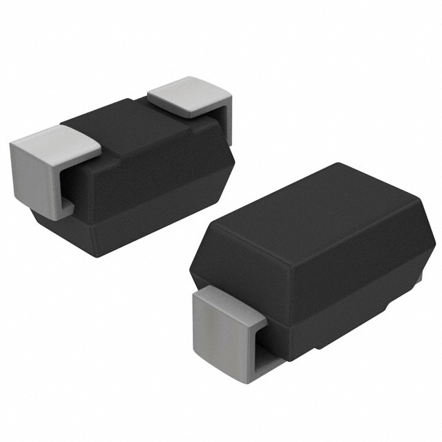
increasingly smaller electronic components. Bourns offers Glass Passivated Rectifiers for rectification applications, in compact chip
DO-214AC (SMA) size format, which offer PCB real estate savings and are considerably smaller than most competitive parts. The Glass
Passivated Rectifier Diodes offer a forward current of 1.0 A with a choice of repetitive peak reverse voltage of 50 V up to 600 V.
Bourns® Chip Diodes conform to JEDEC standards, are easy to handle on standard pick and place equipment and their flat configuration
minimizes roll away.
Electrical Characteristics (@ TA = 25 °C Unless Otherwise Noted)
Parameter
Symbol
Maximum Repetitive
Peak Reverse Voltage
Maximum RMS Voltage
Maximum DC Blocking Voltage
Maximum Average Forward
Rectified Current1
CD214A-
Unit
F150
F1100
F1150
F1200
F1400
F1600
VRRM
50
100
150
200
400
600
V
VRMS
35
70
105
140
280
420
V
VDC
50
100
150
200
400
600
V
E
T
E
L
O
S
B
O
I(AV)
1.0
A
DC Reverse Current @ Rated DC
Blocking Voltage (@TA = 25 °C)
IR
5.0
μA
DC Reverse Current @ Rated DC
Blocking Voltage (@TA = 125 °C)
IR
50.0
μA
Typical Junction Capacitance
CJ
10
pF
Maximum Instantaneous
Forward Voltage @ 1 A
Typical Thermal Resistance
2
VF
3
0.95
1.25
RθJA
1.7
34
V
°C/W
Peak forward surge current 8.3 ms
single half sine-wave superimposed
on rated load (JEDEC Method)
IFSM
30
25
A
Maximum Reverse Recovery Time 4
Trr
25
35
ns
Typical Reverse Recovery Time 4
Trr
20
30
ns
Notes:
1 See Forward Derating Curve.
2 Measured at 1 MHz and an applied reverse voltage of 4.0 V.
3 Thermal resistance from junction to ambient and from junction to lead P.C.B. mounted on 0.2 x 0.2 ˝ (5.0 x 5.0 mm) copper pad areas.
4 Reverse recovery test condition: IF 0.5 A, IR = 1.0 A, Irr = 0.25 A.
Thermal Characteristics (@ TA = 25 °C Unless Otherwise Noted)
Parameter
Operating Temperature Range
Storage Temperature Range
Symbol
CD214A-F150~F1600
Unit
TJ
-55 to +150
°C
TSTG
-55 to +150
°C
WARNING Cancer and Reproductive Harm
www.P65Warnings.ca.gov
*RoHS Directive 2015/863, Mar 31, 2015 and Annex.
Specifications are subject to change without notice. Users should verify actual device performance in their specific
applications. The products described herein and this document are subject to specific legal disclaimers as set forth on the
last page of this document, and at www.bourns.com/docs/legal/disclaimer.pdf.
�CD214A-F150~F1600 Fast Response Rectifiers
Product Dimensions
Recommended Pad Layout
This is an RoHS compliant product using 100 % Sn termination. It
is a molded plastic package. A cathode band indicates the polarity.
The package weighs approximately 0.064 g. The package and
dimensions are shown below.
2.69
MAX.
(0.106)
4.00 - 4.60
(0.160 - 0.180)
2.10
MIN.
(0.083)
1.27 - 1.63
(0.05 - 0.064)
2.29 - 2.92
(0.090 - 0.115)
E
T
E
L
O
S
B
O
DIMENSIONS:
1.27
MIN.
(0.050)
MM
(INCHES)
How To Order
2.00 - 2.43
(0.079 - 0.103)
0.05 - 0.20
(0.002 - 0.008)
0.76 - 1.27
(0.03 - 0.06)
4.83 - 5.59
(0.190 - 0.220)
DIMENSIONS:
MM
(INCHES)
0.15 - 0.31
(0.006 - 0.012)
CD 214A - F 1 400
Common Code
CD = Chip Diode
Package
214A = DO214AC
Model Series
F = Fast Response
Forward Current
1=1A
Reverse Voltage
50 = 50 V
100 = 100 V
150 = 150 V
200 = 200 V
400 = 400 V
600 = 600 V
Typical Part Marking
CD214A-F150 ............................................................................
CD214A-F1100 ..........................................................................
CD214A-F1150 ..........................................................................
CD214A-F1200 ..........................................................................
CD214A-F1400 ..........................................................................
CD214A-F1600 ..........................................................................
F1A
F1B
F1C
F1D
F1G
F1J
Specifications are subject to change without notice.
Users should verify actual device performance in their specific applications.
The products described herein and this document are subject to specific legal disclaimers as set forth on the last page of this document, and at www.bourns.com/docs/legal/disclaimer.pdf.
�CD214A-F150~F1600 Fast Response Rectifiers
Performance Graphs
Maximum Non-Repetitive Surge Current
Forward Current Derating Curve
Peak Forward Surge Current (Amps)
Average Forward Current (Amps)
1.0
0.5
Resistive or
Inductive Load
50
25
20
F1100-F1400
F1600
15
10
Pulse Width 8.3 ms
Single Half Sine-Wave
(JEDEC Method)
5
E
T
E
L
O
S
B
O
0
0
30
70
90
110
130
150
170
0
1
10
Ambient Temperature (°C)
100
Number of Cycles at 60 Hz
Typical Forward Characteristics
Typical Reverse Characteristics
100
10.00
F50-F100
1.00
Instantaneous Reverse Leakage Current (mA)
Instantaneous Forward Current (Amps)
F600
F200F400
0.10
Pulsewidth: 300 µs
1% Duty Cycle
10
1.0
TJ = 125 °C
TJ = 100 °C
0.1
0.01
0.2
0.6
1.0
1.4
1.8
0
2.2
20
40
60
80
100 110
Percent of Rated Peak Reverse Voltage (%)
Instantaneous Forward Voltage (Volts)
Typical Junction Capacitance
200
100
Junction Capacitance (pF)
60
40
20
10
6
4
TJ = 25 °C
2
1
0.1
0.2
0.4
1.0
2
4
10
Reverse Voltage (Volts)
20
40
100
Specifications are subject to change without notice.
Users should verify actual device performance in their specific applications.
The products described herein and this document are subject to specific legal
disclaimers as set forth on the last page of this document, and at
www.bourns.com/docs/legal/disclaimer.pdf.
�CD214A-F150~F1600 Fast Response Rectifiers
Packaging Information
The surface mount product is packaged in a 12 mm x 4 mm tape and reel format per EIA-481 standard.
P
0
P
1
d
T
E
Index Hole
120
F
D2
W
B
D1 D
P
A
Trailer
.......
.......
End
C
E
T
E
L
O
S
B
O
Device
.......
.......
.......
.......
Leader
.......
.......
DIMENSIONS:
10 pitches (min.)
W1
Start
10 pitches (min.)
MM
(INCHES)
Direction of Feed
Item
Symbol
Carrier Width
A
Carrier Length
B
Carrier Depth
C
Sprocket Hole
d
Reel Outside Diameter
D
Reel Inner Diameter
D1
Feed Hole Diameter
D2
Sprocket Hole Position
E
Punch Hole Position
F
Punch Hole Pitch
P
Sprocket Hole Pitch
P0
Embossment Center
P1
Overall Tape Thickness
T
Tape Width
W
Reel Width
W1
Quantity per Reel
—
DO-214AC (SMA)
3.42 ± 0.10
(0.134 ± 0.004)
5.07 ± 0.10
(0.199 ± 0.004)
3.10 ± 0.10
(0.122 ± 0.004)
1.55 ± 0.05
(0.061 ± 0.002)
330
(12.992)
50.0
Min.
(1.969)
13.0 ± 0.50
(0.512 ± 0.020)
1.75 ± 0.10
(0.069 ± 0.004)
5.50 ± 0.50
(0.217 ± 0.020)
4.00 ± 0.10
(0.157 ± 0.004)
4.00 ± 0.10
(0.157 ± 0.004)
2.00 ± 0.05
(0.079 ± 0.002)
0.30 ± 0.10
(0.012 ± 0.004)
12.00 ± 0.20
(0.420 ± 0.008)
18.7
Max.
(0.736)
7,500
Asia-Pacific:
Tel: +886-2 2562-4117
Email: asiacus@bourns.com
Europe:
Tel: +36 88 885 877
Email: eurocus@bourns.com
The Americas:
Tel: +1-951 781-5500
Email: americus@bourns.com
www.bourns.com
REV. 06/21
Specifications are subject to change without notice.
Users should verify actual device performance in their specific applications.
The products described herein and this document are subject to specific legal
disclaimers as set forth on the last page of this document, and at
www.bourns.com/docs/legal/disclaimer.pdf.
�Legal Disclaimer Notice
This legal disclaimer applies to purchasers and users of Bourns® products manufactured by or on behalf of Bourns, Inc. and
P[Z�HɉSPH[LZ��JVSSLJ[P]LS`��¸)V\YUZ¹��
Unless otherwise expressly indicated in writing, Bourns® products and data sheets relating thereto are subject to change
^P[OV\[�UV[PJL���
很抱歉,暂时无法提供与“CD214A-F1100”相匹配的价格&库存,您可以联系我们找货
免费人工找货