T
PL
IA
N
OM
C
*R
oH
S
Features
Applications
n RoHS compliant*
n Switch Mode Power Supplies
n Low profile
n Portable equipment batteries
n Low power loss, high efficiency
n High frequency rectification
n UL 94V-0 classification
n DC/DC Converters
LE
AD
F
RE
E
n Telecommunications
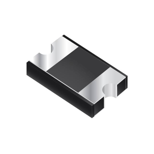
CD214B-B2xR Series Schottky Barrier Rectifier Chip Diode
General Information
Ro VE LEA
HS RS D
C ION FRE
OM S E
PL AR
IA E
NT
*
Portable communications, computing and video equipment manufacturers are
challenging the semiconductor industry to develop increasingly smaller electronic
components.
Bourns offers Schottky Rectifier Diodes for rectification applications, in a compact chip
package compatible with DO-214AA (SMB) size format, which offer PCB real estate
savings and are considerably smaller than competitive parts. The Schottky Rectifier
Diodes offer a forward current of 2 A with a choice of repetitive peak reverse voltage of
20 V up to 100 V.
Absolute Maximum Ratings (@ TA = 25 °C Unless Otherwise Noted)
Parameter
Symbol
Maximum Repetitive Peak Reverse Voltage
Maximum Average Forward Current
Maximum Peak Forward Surge Current
(8.3 ms Single Half Sine-Wave)
Operating Junction Temperature Range
VRRM
B240R
40
CD214B-
B260R
60
B2100R
100
Unit
V
IF(AV)
2
A
IFSM
50
A
TOPR
Storage Temperature Range
B220R
20
-55 to +125
TSTG
-55 to +150
°C
-55 to +150
°C
Electrical Characteristics (@ TA = 25 °C Unless Otherwise Noted)
Parameter
Symbol
IF = 1 A
Maximum Instantaneous
Forward Voltage (NOTE 1)
VF
IF = 2 A
DC Reverse Current
Typical Junction Capacitance
Typical
Thermal
Resistance
(NOTE 2)
IR
CJ
Condition or Model
CD214B-B220R
CD214B-B240R
CD214B-B260R
CD214B-B2100R
CD214B-B220R
CD214B-B240R
CD214B-B260R
CD214B-B2100R
VR = VRRM
VR = 4 V, f = 1.0 MHz
Min.
Typ.
Max.
Unit
0.41
0.5
0.62
0.49
0.5
0.6
0.75
0.025
115
0.7
0.85
0.2
Junction to
Ambient
RθJA
65
Junction to
Lead
RθJL
17
NOTES:
(1) Pulse width 300 microsecond, 1 % duty cycle.
(2) Mounted on PCB with 5.0 x 5.0 mm (0.2 x 0.2 inch) copper pad areas.
*RoHS Directive 2015/863, Mar 31, 2015 and Annex.
Specifications are subject to change without notice.
The device characteristics and parameters in this data sheet can and do vary in different applications and actual device performance may vary over time.
Users should verify actual device performance in their specific applications.
V
mA
pF
°C/W
� CD214B-B2xR
3312 - 2 mm
SMD
Trimming
Potentiometer
Series
Schottky
Barrier Rectifier
Chip Diode
Performance Graphs
Max. Peak Forward Surge Current
Average Forward Rectified Current
(Amps)
Forward Current Derating Curve
60
Peak Forward Surge Current
(Amps)
2.0
CD214B-B260R
CD214B-B2100R
CD214B-B220R
CD214B-B240R
1.0
0
Resistive or
Inductive Load
PCB Mounted on
5.0 x 5.0 mm
(0.2 x 0.2 inch)
Copper Pad Areas
0
50
70
90
110
130
150
50
40
(JEDEC Method)
30
20
10
0
170
8.3 ms
Single Half
Sine-Wave
0
Lead Temperature (°C)
Typical Instantaneous Forward Characteristics
100
CD214B-B260R
Instantaneous Reverse Current (mA)
Instantaneous Forward Current (A)
100
Typical Reverse Characteristics
10
CD214B-B220R
CD214B-B240R
1
CD214B-B2100R
0.1
0.01
Ta = 25 °C
0.001
10
Number of Cycles @ 60 Hz
0
0.1
0.2
0.3
0.4
0.5
0.6
0.7
0.8
10
TJ = 100 °C
1
0.1
0.01
TJ = 25 °C
0.001
0
20
40
60
Typical Junction Capacitance
Junction Capacitance (pF)
400
100
TJ = 25 °C
f = 1.0 MHz
Vsig = 50 mVP-P
10
0.1
1.0
10
80
100
Percent of Rated Peak Reverse Voltage (%)
Instantaneous Forward Voltage (Volts)
100
Reverse Voltage (Volts)
Specifications are subject to change without notice.
The device characteristics and parameters in this data sheet can and do vary in different applications and actual device performance may vary over time.
Users should verify actual device performance in their specific applications.
�
3312 - 2 mmSeries
SMDSchottky
Trimming
Potentiometer
CD214B-B2xR
Barrier
Rectifier Chip Diode
Product Dimensions
Recommended Pad Layout
A
A
G
G
B
D
DIA.
C
B
C
D
DIA.
H
H
I
I
E
E
E
E
Dimension
CD214B-B2 Series
G
2.65 MAX.
(0.104)
H
3.00 MIN.
(0.118)
I
6.65 REF.
(0.262)
F
F
Dimension
CD214B-B2 Series
A
5.20 ± 0.10
(0.205 ± 0.004)
B
3.60 ± 0.10
(0.142 ± 0.004)
C
3.01 TYP.
TYP.
(0.119)
D (Dia.)
0.695 ± 0.015
(0.027 ± 0.001)
E
1.15 ± 0.1
(0.045 ± 0.004)
F
1.10 ± 0.15
(0.043 ± 0.006)
MM
DIMENSIONS:
(INCHES)
Typical Part Marking
DATE CODE:
Y = LAST
DIGIT OF
YEAR
WW = WEEK
NUMBER
202
YWW
DEVICE CODE:
202 = CD214B-B220R
204 = CD214B-B240R
206 = CD214B-B260R
210 = CD214B-B2100R
MM
DIMENSIONS:
(INCHES)
Environmental Specifications
Moisture Sensitivity Level.................................................................1
ESD Classification (HBM)............................................................. 3B
How to Order
CD 214B - B 2 20 R
Common Code
CD = Chip Diode
Package
214B = SMB/DO-214AA Compatible
Model
B = Schottky Barrier Series
Maximum Average Forward Rectified Current
2=2A
Maximum Repetitive Peak Reverse Voltage
20 = 20 V
40 = 40 V
60 = 60 V
100 = 100 V
Specifications are subject to change without notice.
The device characteristics and parameters in this data sheet can and do vary in different applications and actual device performance may vary over time.
Users should verify actual device performance in their specific applications.
�
3312 - 2 mmSeries
SMDSchottky
Trimming
Potentiometer
CD214B-B2xR
Barrier
Rectifier Chip Diode
Packaging Information
The product is dispensed in tape and reel format (see diagram below).
P
0
P
1
d
T
E
Index Hole
120 °
F
D1 D
P
A
Trailer
End
D2
W
B
.......
.......
C
Device
.......
.......
Leader
.......
.......
.......
.......
30 pitches
Start
W1
MM
DIMENSIONS:
(INCHES)
30 pitches
Direction of Feed
Item
Symbol
CD214B-B2 Series
Carrier Width
A
3.70 ± 0.10
(0.146 ± 0.004)
Carrier Length
B
5.40 ± 0.10
(0.213 ± 0.004)
Carrier Depth
C
1.65 ± 0.10
(0.065 ± 0.004)
Sprocket Hole
d
1.50 ± 0.10
(0.059 ± 0.004)
Reel Outside Diameter
D
330 ± 2.0
(12.992 ± 0.079)
Reel Inner Diameter
D1
50.0
MIN.
(1.969)
D2
13.0 ± 0.50
(0.512 ± 0.020)
Sprocket Hole Position
E
1.75 ± 0.10
(0.069 ± 0.004)
Punch Hole Position
F
5.50 ± 0.05
(0.217 ± 0.002)
Punch Hole Pitch
P
8.00 ± 0.10
(0.157 ± 0.004)
Sprocket Hole Pitch
P0
4.00 ± 0.10
(0.157 ± 0.004)
Embossment Center
P1
2.00 ± 0.10
(0.079 ± 0.004)
Feed Hole Diameter
Overall Tape Thickness
T
Tape Width
W
Reel Width
W1
Quantity per Reel
--
Asia-Pacific:
Tel: +886-2 2562-4117
Email: asiacus@bourns.com
Europe:
Tel: +36 88 520 390
Email: eurocus@bourns.com
The Americas:
Tel: +1-951 781-5500
Email: americus@bourns.com
www.bourns.com
0.40
MAX.
(0.016)
12.00 ± 0.30
(0.472 ± 0.012)
18.7
MAX.
(0.736)
5,000
01/18
Specifications are subject to change without notice.
The device characteristics and parameters in this data sheet can and do vary in different applications and actual device performance may vary over time.
Users should verify actual device performance in their specific applications.
�
很抱歉,暂时无法提供与“CD214B-B260R”相匹配的价格&库存,您可以联系我们找货
免费人工找货- 国内价格 香港价格
- 10000+1.5111510000+0.19549