T
PL
IA
N
M
CO
*R
oH
S
Features
Applications
■ RoHS compliant*
■ Switch Mode Power Supplies
■ Low profile
■ Portable equipment batteries
■ Low power loss, high efficiency
■ High frequency rectification
■ UL 94V-0 classification
■ DC/DC Converters
■ Telecommunications
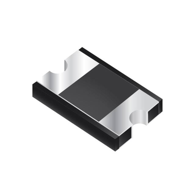
CD214C-FS3x Series Fast Response Rectifier Chip Diode
General Information
Portable communications, computing and video equipment manufacturers are challenging the
semiconductor industry to develop increasingly smaller electronic components.
Bourns offers Glass Passivated Rectifiers for rectification applications in a compact chip
package compatible with DO-214AB (SMC) size format. The Glass Passivated Rectifier
Diodes offer a forward current of 3 A with a choice of repetitive peak reverse voltage of 200 V
up to 600 V.
Absolute Maximum Ratings (@ TA = 25 °C Unless Otherwise Noted)
Parameter
Symbol
FS3D
200
CD214CFS3G
400
Unit
FS3J
600
Maximum Repetitive Peak Reverse Voltage
VRRM
Maximum Average Forward Current
IF(AV)
3
V
A
Maximum Peak Forward Surge Current
(8.3 ms Single Half Sine-Wave)
IFSM
100
A
Operating Junction Temperature Range
TOPR
-65 to +175
°C
Storage Temperature Range
TSTG
-65 to +175
°C
Electrical Characteristics (@ TA = 25 °C Unless Otherwise Noted)
Parameter
Symbol
Maximum Instantaneous Forward Voltage
(NOTE 1)
DC Reverse Current
Reverse Recovery Time
IR
IF= 0.5 A,
IR = 1.0 A,
Irr = 0.25 A
Typical Junction Capacitance
Typical Thermal Resistance
(NOTE 2)
VF
Trr
CJ
Junction to
Ambient
Junction to
Lead
Condition or Model
CD214C-FS3D
IF = 3 A
CD214C-FS3G
CD214C-FS3J
VR =
VRRM
VR = 4 V, f = 1.0 MHz
Min.
Typ.
0.93
1.2
1.4
Max.
0.95
1.25
1.7
Unit
0.2
5
μA
V
35
nS
19
pF
RθJA
60
RθJL
10
°C/W
NOTES:
(1) Pulse width 300 microsecond, 1 % duty cycle.
(2) Mounted on PCB with 5.0 x 5.0 mm (0.2 x 0.2 inch) copper pad areas.
WARNING Cancer and Reproductive Harm - www.P65Warnings.ca.gov
*RoHS Directive 2015/863, Mar 31, 2015 and Annex.
Specifications are subject to change without notice.
Users should verify actual device performance in their specific applications.
The products described herein and this document are subject to specific legal disclaimers as set forth on the last page of this document, and at www.bourns.com/docs/legal/disclaimer.pdf.
�CD214C-FS3x Series Fast Response Rectifier Chip Diode
Performance Graphs
Maximum Peak Forward Surge Current
120
3.0
Peak Forward Surge Current
(Amps)
Average Forward Rectified Current
(Amps)
Forward Current Derating Curve
2.5
2.0
1.5
Resistive or
Inductive Load
PCB Mounted on
5.0 x 5.0 mm
(0.2 x 0.2 inch)
Copper Pad Areas
1.0
0.5
0
0
25
100
125
150
8.3 ms
Single Half
Sine-Wave
80
(JEDEC Method)
60
40
20
0
75
50
100
175
0
10
Typical Instantaneous Forward Characteristics
Typical Reverse Characteristics
100
Instantaneous Reverse Current (mA)
10
Instantaneous Forward Current (A)
100
Number of Cycles @ 60 Hz
Lead Temperature (°C)
CD214C-FS3G
CD214C-FS3D
CD214C-FS3J
1
0.1
Ta = 25 °C
C
TJ = 150 °C
10
1
0.1
0.01
0.01
0.2
0.6
1.0
1.4
1.8
2.2
TJ = 125 °C
TJ = 25 °C
0
20
40
60
80
100 110
Percent of Rated Peak Reverse Voltage (%)
Instantaneous Forward Voltage (Volts)
Junction Capacitance (pF)
Typical Junction Capacitance
200
100
60
40
20
10
6
4
2
1
0.1
TJ = 25 °C
f = 1.0 MHz
Vsig = 50 mVP-P
0.1
0.4
1
2
4
10
20
40
100
Reverse Voltage (Volts)
Specifications are subject to change without notice.
Users should verify actual device performance in their specific applications.
The products described herein and this document are subject to specific legal disclaimers as set forth on the last page of this document, and at www.bourns.com/docs/legal/disclaimer.pdf.
�CD214C-FS3x Series Fast Response Rectifier Chip Diode
Product Dimensions
Recommended Pad Layout
A
G
B
D
C
H
I
E
E
F
Dimension
CD214C-FS Series
A
8.0 ± 0.10
(0.315 ± 0.004)
B
5.0 ± 0.10
(0.197 ± 0.004)
C
3.90 TYP.
(0.154)
D
0.80 ± 0.02
(0.031 ± 0.001)
E
1.95 ± 0.10
(0.077 ± 0.004)
F
1.10 ± 0.15
(0.043 ± 0.006)
DIMENSIONS:
MM
(INCHES)
Dimension
CD214C-FS Series
G
4.10 MAX.
(0.161)
H
3.90 MIN.
(0154)
I
11.90 REF.
(0.469)
DIMENSIONS:
MM
(INCHES)
Environmental Specifications
Moisture Sensitivity Level ................................................................1
ESD Classification (HBM)............................................................. 3B
Typical Part Marking
DEVICE CODE:
FS3D = CD214C-FS3D
FS3G = CD214C-FS3G
FS3J = CD214C-FS3J
DATE CODE:
Y = LAST
DIGIT OF
YEAR
WW = WEEK
NUMBER
FS3D
YWW
How to Order
CD 214C - FS 3 D
Common Code
CD = Chip Diode
Package
214C = SMC/DO-214AB Compatible
Model
FS = Fast Response Rectifier
Maximum Average Forward Rectified Current
3=3A
Maximum Repetitive Peak Reverse Voltage
D = 200 V
G = 400 V
J = 600 V
Specifications are subject to change without notice.
Users should verify actual device performance in their specific applications.
The products described herein and this document are subject to specific legal disclaimers as set forth on the last page of this document, and at www.bourns.com/docs/legal/disclaimer.pdf.
�CD214C-FS3x Series Fast Response Rectifier Chip Diode
Packaging Information
The product is dispensed in tape and reel format (see diagram below).
P
0
P
1
d
T
E
Index Hole
120 °
F
D2
W
B
D1 D
P
A
Trailer
End
.......
.......
C
Device
.......
.......
Leader
.......
.......
.......
.......
30 pitches
W1
Start
DIMENSIONS:
MM
(INCHES)
30 pitches
Direction of Feed
Item
Symbol
CD214C-FS3 Series
Carrier Width
A
5.56 ± 0.10
(0.219 ± 0.004)
Carrier Length
B
8.18 ± 0.10
(0.322 ± 0.004)
Carrier Depth
C
Sprocket Hole
d
1.55 ± 0.05
(0.061 ± 0.002)
Reel Outside Diameter
D
330 ± 2.0
(12.992 ± 0.079)
Reel Inner Diameter
D1
Feed Hole Diameter
D2
13.0 ± 0.50
(0.512 ± 0.020)
Sprocket Hole Position
E
1.75 ± 0.10
(0.069 ± 0.004)
Punch Hole Position
F
7.50 ± 0.10
(0.295 ± 0.004)
Punch Hole Pitch
P
8.00 ± 0.10
(0.315 ± 0.004)
Sprocket Hole Pitch
P0
4.00 ± 0.10
(0.157 ± 0.004)
Embossment Center
P1
2.00 ± 0.10
(0.079 ± 0.004)
Overall Tape Thickness
T
Tape Width
W
Reel Width
W1
Quantity per Reel
--
2.50
MAX.
(0.098)
50.0
MIN.
(1.969)
0.40
MAX.
(0.016)
16.00 ± 0.30
(0.630 ± 0.012)
22.7
MAX.
(0.893)
3,000
Asia-Pacific:
Tel: +886-2 2562-4117
Email: asiacus@bourns.com
Europe:
Tel: +36 88 885 877
Email: eurocus@bourns.com
The Americas:
Tel: +1-951 781-5500
Email: americus@bourns.com
www.bourns.com
REV. 08/19
Specifications are subject to change without notice.
Users should verify actual device performance in their specific applications.
The products described herein and this document are subject to specific legal
disclaimers as set forth on the last page of this document, and at
www.bourns.com/docs/legal/disclaimer.pdf.
�Legal Disclaimer Notice
This legal disclaimer applies to purchasers and users of Bourns® products manufactured by or on behalf of Bourns, Inc. and
P[Z�HɉSPH[LZ��JVSSLJ[P]LS`��¸)V\YUZ¹��
Unless otherwise expressly indicated in writing, Bourns® products and data sheets relating thereto are subject to change
^P[OV\[�UV[PJL���
很抱歉,暂时无法提供与“CD214C-FS3D”相匹配的价格&库存,您可以联系我们找货
免费人工找货- 国内价格
- 1+4.54924
- 10+3.18495
- 100+2.80405
- 250+2.34889
- 1000+2.11651
- 3000+1.98715
- 6000+1.89372
- 国内价格 香港价格
- 9000+1.630079000+0.21060
- 国内价格 香港价格
- 1+4.898131+0.63280
- 10+3.4286910+0.44296
- 100+3.01760100+0.38985
- 250+2.52779250+0.32657
- 1000+2.274141000+0.29380
- 3000+2.134193000+0.27572
- 6000+2.037986000+0.26329