PL
IA
N
T
Features
This series is currently available, but
not recommended for new designs.
The Model CD123D-B Series is the
recommended replacement.
OM
n RoHS compliant*
*R
oH
S
C
n Low profile
n Surface mount
LE
AD
F
RE
E
n Very low forward voltage drop
CD216A-B120L~B140 MITE Chip Diode
General Information
Ro VE LEA
HS RS D
C ION FRE
OM S E
PL AR
IA E
NT
*
The markets of portable communications, computing and video equipment are challenging the semiconductor industry to develop increasingly
smaller electronic components.
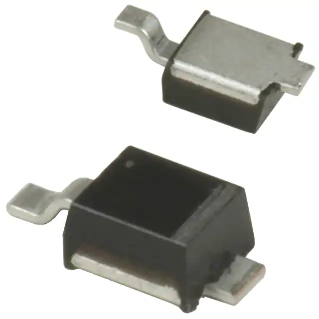
Bourns offers Schottky Rectifier Diodes for rectification applications in compact DO-216AA size chip package formats, which offer PCB real
estate savings and are considerably smaller than competitive parts. The Schottky Barrier Rectifier Diodes offer a forward current of 1 A with a
choice of repetitive peak reverse voltage of 20 V up to 40 V.
Bourns® Chip Diodes conform to JEDEC standards, are easy to handle with standard pick and place equipment and their flat configuration
minimizes roll away.
Electrical Characteristics (@ TA = 25 °C Unless Otherwise Noted)
Parameter
Forward Voltage (Max.) (lf = 1 A)
Typical Junction Capacitance**
Reverse Current (Max.) (@ Rated VR)
Symbol
VF
CT
IR
B120L
0.45
90
400
CD216B120R
B130L
0.53
0.38
75
70
10
410
B140
0.55
60
500
Unit
V
pF
µA
**Measured at 1.0 MHz and applied reverse voltage of 4.0 V DC.
Absolute Ratings (@ TA = 25 °C Unless Otherwise Noted)
Parameter
Repetitive Peak Reverse Voltage
DC Blocking Voltage
RMS Voltage
Average Forward Current @ TL = 130 °C
Peak Forward Surge Current***
Max. Instantaneous Forward Voltage****
@ IF = 0.1 A
@ IF = 1.0 A
@ IF = 2.0 A
@ IF = 3.0 A
Max. Instantaneous Reverse Current
@ VR = 40 V
@ VR = 30 V
@ VR = 20 V
@ VR = 10 V
@ VR = 5 V
Thermal Resistance
Junction to Lead (Anode)
Junction to Tab (Cathode)
Junction to Ambient
Storage Temperature
Junction Temperature
Symbol
VRRM
VDC
VRMS
IO
IFSM
VF
B120L
20
20
14
50
0.34
0.45
0.65
IR
0.4
0.1
RƟJL
RƟJTAB
RƟJA
TSTG
TJ
CD216B120R
B130L
20
30
20
30
14
21
1
50
50
0.455
0.53
0.595
0.0100
0.0010
0.0005
B140
40
40
28
Unit
40
V
V
V
A
A
0.30
0.38
0.36
0.55
V
0.52
0.85
0.41
0.13
0.05
35
20
250
-55 to +150
-55 to +125
0.50
0.15
mA
°C/W
°C
°C
***Surge Current 8.3 ms single phase, half sine wave, 60 Hz (JEDEC Method).
****Pulse Test; Pulse Width = 300 µS, Duty Cycle = 2 %.
*RoHS Directive 2002/95/EC Jan. 27, 2003 including annex and RoHS Recast 2011/65/EU June 8, 2011.
Specifications are subject to change without notice.
Users should verify actual device performance in their specific applications.
The products described herein and this document are subject to specific disclaimers as set forth on the last page of this document, and at www.bourns.com/legal/disclaimer.pdf.
�Applications
n Cellular phones
n PDAs
n Desktop PCs and notebooks
n Digital cameras
n MP3 players
CD216A-B120L~B140 MITE Chip Diode
Product Dimensions
Recommended Pad Layout
H
TAB
1
A
TAB
1
A
K
B
K
C
A
H
B
J
B
C
B
D
J
I
G
E
I
G
F
G
Dimension
DO-216AA
A
1.75 - 2.05
(0.069 - 0.081)
B
1.80 - 2.20
(0.071 - 0.087)
CATHODE C CATHODE
TAB 1
TAB 1
0.95 - 1.15
ANODE
(0.037 - 0.045)
TAB 2
D
0.42 - 0.68
(0.017 - 0.027)
E
0.70 - 1.00
(0.028 - 0.039)
F
0.05 - 0.10
(0.002 - 0.004)
G
0.10 - 0.25
(0.004 - 0.010)
H
3.65 - 3.95
(0.144 - 0.156)
I
0.40 - 0.70
(0.016 - 0.028)
J
1.10 - 1.50
(0.043 - 0.059)
K
0.20 - 0.80
(0.008 - 0.060)
MM
DIMENSIONS:
(INCHES)
D
E
DO-216AA
A
2.67
(0.105)
B
2.54
(0.100)
C
1.27
(0.050)
D
0.625
(0.025)
E
0.762
(0.030)
F
E
D
D
Dimension
C
G
A
C
E
Physical Specifications
Case.............................................. JEDEC 20-216AA Molded plastic
Polarity...............................................Cathode designated by TAB 1
Weight....................................................Approximately 0.016 grams
Mounting Position................................................................ One way
Typical Part Marking
ANODE
TAB 2
CD216A-B120L........................................................................... B2L
CD216A-B120R...........................................................................B2E
CD216A-B130L........................................................................... B3L
CD216A-B140.............................................................................B4S
How to Order
CD 216A - B 1 20 L LF
Common Code
Chip Diode
Package
• 216A = DO-216AA
Model
B = Schottky Barrier Series
Average Forward Current (IO) Code
1 = 1 A (Code x 1000 mA = Average Forward Current)
Reverse Voltage (VR) Code
20 = 20 V
30 = 30 V
40 = 40 V
Forward Voltage Suffix
L = Low Forward Voltage Vf (CD216-B120L, CD216-B130L)
R = Low Leakage Current IR (CD216-B120R)
Terminations
LF = 100 % Sn (RoHS Compliant)
Specifications are subject to change without notice.
Users should verify actual device performance in their specific applications.
The products described herein and this document are subject to specific disclaimers as set forth on the last page of this document, and at www.bourns.com/legal/disclaimer.pdf.
�
CD216A-B120L~B140 MITE Chip Diode
Rating & Characteristic Curves: CD216A-B120L
Forward Characteristics
Reverse Characteristics
10
100
Ta = 25 °C
Pulsewidth: 300 µs
125 °C
10
Reverse Current (µA)
Forward Current (Amps)
100 °C
1
1
0.1
25 °C
0.01
0.1
125 °C
100 °C
0.0
0.001
25 °C
0.2
0.4
0.6
0
0.8
5
10
15
20
25
Reverse Voltage (Volts)
Forward Voltage (Volts)
Derating Curve
Capacitance Between Terminals
1.25
200
180
F = 1 MHz
Ta = 25 ϒC
160
140
0.75
Capacitance (pF)
Average Forward Current (Amps)
1.00
0.50
100
80
60
0.25
Single Phase Half Wave 60 Hz
Resistive or Inductive Load
0.00
120
25
50
75
40
100
Lead Temperature (ϒC)
125
150
20
0
0
10
20
30
40
Reverse Voltage (Volts)
Specifications are subject to change without notice.
Users should verify actual device performance in their specific applications.
The products described herein and this document are subject to specific disclaimers as set forth on the last page of this document, and at www.bourns.com/legal/disclaimer.pdf.
�
CD216A-B120L~B140 MITE Chip Diode
Rating & Characteristic Curves: CD216A-B120R
Forward Characteristics
Reverse Characteristics
10
1000
Ta = 25 °C
Pulsewidth: 300 µs
125 °C
100
Reverse Current (µA)
Forward Current (Amps)
100 °C
1
10
1
25 °C
0.1
0.1
125 °C
100 °C
0.2
0.01
25 °C
0.4
0.6
0
5
10
0.8
15
20
25
Reverse Voltage (Volts)
Forward Voltage (Volts)
Capacitance Between Terminals
1.25
150
1.00
125
F = 1 MHz
Ta = 25 ϒC
100
0.75
Capacitance (pF)
Average Forward Current (Amps)
Derating Curve
0.50
75
50
0.25
Single Phase Half Wave 60 Hz
Resistive or Inductive Load
0.00
25
50
75
25
100
Lead Temperature (ϒC)
125
150
0
0
10
20
30
40
Reverse Voltage (Volts)
Specifications are subject to change without notice.
Users should verify actual device performance in their specific applications.
The products described herein and this document are subject to specific disclaimers as set forth on the last page of this document, and at www.bourns.com/legal/disclaimer.pdf.
�
CD216A-B120L~B140 MITE Chip Diode
Rating & Characteristic Curves: CD216A-B130L
Forward Characteristics
Reverse Characteristics
10
100
Ta = 25 °C
Pulsewidth: 300 µs
125 °C
10
Reverse Current (µA)
Forward Current (Amps)
100 °C
1
1
0.1
25 °C
0.01
100 °C
0.1
125 °C
0
0.001
25 °C
0.2
0.4
0.6
0.8
0
5
10
1
15
20
25
30
35
Reverse Voltage (Volts)
Forward Voltage (Volts)
Capacitance Between Terminals
1.25
150
1.00
125
F = 1 MHz
Ta = 25 ϒC
100
0.75
Capacitance (pF)
Average Forward Current (Amps)
Derating Curve
0.50
75
50
0.25
Single Phase Half Wave 60 Hz
Resistive or Inductive Load
0.00
25
50
75
25
100
Lead Temperature (ϒC)
125
150
0
0
10
20
30
40
Reverse Voltage (Volts)
Specifications are subject to change without notice.
Users should verify actual device performance in their specific applications.
The products described herein and this document are subject to specific disclaimers as set forth on the last page of this document, and at www.bourns.com/legal/disclaimer.pdf.
�
CD216A-B120L~B140 MITE Chip Diode
Rating & Characteristic Curves: CD216A-B140
Forward Characteristics
Reverse Characteristics
10
10
Ta = 25 °C
Pulsewidth: 300 µs
125 °C
1
Reverse Current (mA)
Forward Current (Amps)
100 °C
1
0.1
0.01
25 °C
0.001
0.0001
0
100 °C
0.1
125 °C
0
0.2
5
10
15
20
25
30
35
40
45
Reverse Voltage (Volts)
25 °C
0.4
0.6
0.8
1
Forward Voltage (Volts)
Capacitance Between Terminals
1.25
150
1.00
125
F = 1 MHz
Ta = 25 ϒC
100
0.75
Capacitance (pF)
Average Forward Current (Amps)
Derating Curve
0.50
75
50
0.25
Single Phase Half Wave 60 Hz
Resistive or Inductive Load
0.00
25
50
75
25
100
Lead Temperature (ϒC)
125
150
0
0
10
20
30
40
Reverse Voltage (Volts)
Specifications are subject to change without notice.
Users should verify actual device performance in their specific applications.
The products described herein and this document are subject to specific disclaimers as set forth on the last page of this document, and at www.bourns.com/legal/disclaimer.pdf.
�
3312 - 2 mm SMD Trimming
CD216A-B120L~B140
MITE ChipPotentiometer
Diode
Packaging Information
The product is dispensed in tape and reel format (see diagram below).
P
0
P
1
d
T
E
Index Hole
Pin 1
Location
120 °
F
D2
W
B
D1 D
P
A
Trailer
.......
.......
End
C
Device
.......
.......
.......
.......
10 pitches (min.)
Leader
.......
.......
Start
10 pitches (min.)
Direction of Feed
Item
Symbol
Carrier Width
A
Carrier Length
B
Carrier Depth
C
Sprocket Hole
d
Reel Outside Diameter
D
Reel Inner Diameter
D1
Feed Hole Diameter
D2
Sprocket Hole Position
E
Punch Hole Position
F
Punch Hole Pitch
P
Sprocket Hole Pitch
P0
Embossment Center
P1
Overall Tape Thickness
T
Tape Width
W
Reel Width
W1
Quantity per Reel
--
W1
MM
DIMENSIONS:
(INCHES)
Devices are packed in accordance with EIA standard
RS-481-A and specifications shown here.
DO-216AA
2.90 ± 0.10
(0.114 ± 0.004)
5.30 ± 0.10
(0.209 ± 0.004)
1.37 ± 0.10
(0.054 ± 0.004)
1.55 ± 0.05
(0.061 ± 0.002)
178
(7.008)
75.0
(2.953) MIN.
13.0 ± 0.20
(0.512 ± 0.008)
1.75 ± 0.10
(0.069 ± 0.004)
5.50 ± 0.05
(0.217 ± 0.002)
4.00 ± 0.10
(0.157 ± 0.004)
4.00 ± 0.10
(0.157 ± 0.004)
2.00 ± 0.05
(0.079 ± 0.002)
0.40 ± 0.10
(0.016 ± 0.004)
12.00 ± 0.20
(0.472 ± 0.008)
18.4
(0.724) MAX.
3,000
REV. 10/17
Specifications are subject to change without notice.
Users should verify actual device performance in their specific applications.
The products described herein and this document are subject to specific disclaimers as set forth on the last page of this document, and at www.bourns.com/legal/disclaimer.pdf.
�
Legal Disclaimer Notice
This legal disclaimer applies to purchasers and users of Bourns® products manufactured by or on behalf of Bourns, Inc. and
its affiliates (collectively, “Bourns”).
Unless otherwise expressly indicated in writing, Bourns® products and data sheets relating thereto are subject to change
without notice. Users should check for and obtain the latest relevant information before placing orders and should verify that
such information is current and complete.
The characteristics and parameters of a Bourns® product set forth in its data sheet are based on laboratory conditions, and
statements regarding the suitability of products for certain types of applications are based on Bourns’ knowledge of typical
requirements in generic applications. The characteristics and parameters of a Bourns® product in a user application may vary
from the data sheet characteristics and parameters due to a combination of the Bourns® product with other components in
the user’s application or due to the environment of the user application itself. Such characteristics and parameters also can
and do vary in different applications and actual performance may vary over time. Users should always verify actual performance
of the Bourns® product in their specific devices and applications, and make their own independent judgments about how
much additional test margin to design in to compensate for differences between laboratory and real world conditions.
Unless Bourns has explicitly designated an individual Bourns® product as meeting the requirements of a particular industry
standard (e.g., ISO/TS 16949) or a particular qualification (e.g., UL listed or recognized), Bourns is not responsible for any
failure of an individual Bourns® product to meet requirements of such industry standard or such particular qualification. Users
of Bourns® products are responsible for ensuring compliance with safety-related requirements and standards applicable to
their applications.
Bourns® products are not recommended, authorized or intended for use in nuclear, lifesaving, life-critical or life-sustaining
applications, nor in any other applications where failure or malfunction may result in personal injury, death, or severe property
or environmental damage. Unless expressly and specifically approved in writing by two authorized Bourns representatives on
a case-by-case basis, use of any Bourns® products in such unauthorized applications is at the user’s sole risk. Life-critical
applications include devices identified by the U.S. Food and Drug Administration as Class III devices and generally equivalent
classifications outside of the United States.
Bourns® standard products that are designed and tested for use in automotive applications will be described on the applicable
data sheets as compliant with the applicable AEC-Q standard. Unless expressly and specifically approved in writing by two
authorized Bourns representatives on a case-by-case basis, use of any other Bourns® standard products in an automotive
application is not recommended, authorized or intended and will be at the user’s sole risk.
Bourns® standard products are not tested to comply with United States Federal Aviation Administration standards generally
or any other generally equivalent governmental organization standard applicable to products designed or manufactured for
use in aircraft or space applications. Bourns® standard products that are designed and tested for use in aircraft or space
applications will be described on the applicable data sheets as compliant with the RTCA DO-160 standard. Unless expressly
and specifically approved in writing by two authorized Bourns representatives on a case-by-case basis, use of any other
Bourns® standard product in an aircraft or space application is not recommended, authorized or intended and will be at the
user’s sole risk.
The use and level of testing applicable to Bourns® custom products shall be negotiated on a case-by-case basis by Bourns
and the user for which such Bourns® custom products are specially designed. Absent a written agreement between Bourns
and the user regarding the use and level of such testing, the provisions above applicable to Bourns® standard products shall
also apply to such Bourns® custom products.
Users shall not sell, transfer, export or re-export any Bourns® products or technology for use in activities which involve the
design, development, production, use or stockpiling of nuclear, chemical or biological weapons or missiles, nor shall they use
Bourns® products or technology in any facility which engages in activities relating to such devices. The foregoing restrictions
apply to all uses and applications that violate national or international prohibitions, including embargos or international
regulations. Further, Bourns® products, technology or technical data may not under any circumstance be exported or
re-exported to countries subject to international sanctions or embargoes, and Bourns® products may not, without prior
authorization from Bourns and/or the U.S. Government, be resold, transferred, or re-exported to any party not eligible to
receive U.S. commodities, software, and technical data.
To the maximum extent permitted by applicable law, Bourns disclaims (i) any and all liability arising out of the application or
use of any Bourns® standard product, (ii) any and all liability, including, without limitation, special, punitive, consequential
or incidental damages, and (iii) any and all implied warranties, including implied warranties of fitness for particular purpose,
non-infringement and merchantability.
For your convenience, copies of this Legal Disclaimer Notice with German, Spanish, Japanese, Traditional Chinese and Simplified Chinese
bilingual versions are available at:
Web Page: http://www.bourns.com/legal/disclaimers-terms-and-policies
PDF: http://www.bourns.com/docs/Legal/disclaimer.pdf
C1753 10/18/17
�