T
PL
IA
N
M
CO
Features
This series is currently available, but
not recommended for new designs.
The Model CD123D-B Series is the
recommended replacement.
■ RoHS compliant*
*R
oH
S
■ Low profile
■ Surface mount
■ Very low forward voltage drop
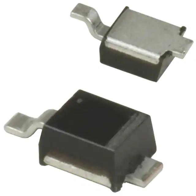
CD216A-B120L~B140 MITE Chip Diode
General Information
The markets of portable communications, computing and video equipment are challenging the semiconductor industry to develop increasingly
smaller electronic components.
Bourns offers Schottky Rectifier Diodes for rectification applications in compact DO-216AA size chip package formats, which offer PCB real
estate savings and are considerably smaller than competitive parts. The Schottky Barrier Rectifier Diodes offer a forward current of 1 A with a
choice of repetitive peak reverse voltage of 20 V up to 40 V.
Bourns® Chip Diodes conform to JEDEC standards, are easy to handle with standard pick and place equipment and their flat configuration
minimizes roll away.
Electrical Characteristics (@ TA = 25 °C Unless Otherwise Noted)
Parameter
Forward Voltage (Max.) (lf = 1 A)
Typical Junction Capacitance**
Reverse Current (Max.) (@ Rated VR)
Symbol
VF
CT
IR
B120L
0.45
90
400
CD216B120R
B130L
0.53
0.38
75
70
10
410
B140
0.55
60
500
Unit
V
pF
μA
**Measured at 1.0 MHz and applied reverse voltage of 4.0 V DC.
Absolute Ratings (@ TA = 25 °C Unless Otherwise Noted)
Parameter
Repetitive Peak Reverse Voltage
DC Blocking Voltage
RMS Voltage
Average Forward Current @ TL = 130 °C
Peak Forward Surge Current***
Max. Instantaneous Forward Voltage****
@ IF = 0.1 A
@ IF = 1.0 A
@ IF = 2.0 A
@ IF = 3.0 A
Max. Instantaneous Reverse Current
@ VR = 40 V
@ VR = 30 V
@ VR = 20 V
@ VR = 10 V
@ VR = 5 V
Thermal Resistance
Junction to Lead (Anode)
Junction to Tab (Cathode)
Junction to Ambient
Storage Temperature
Junction Temperature
Symbol
VRRM
VDC
VRMS
IO
IFSM
VF
B120L
20
20
14
CD216B120R
B130L
20
30
20
30
14
21
1
50
50
B140
40
40
28
Unit
40
V
V
V
A
A
0.30
0.38
0.36
0.55
V
0.65
0.52
0.85
0.4
0.1
0.41
0.13
0.05
50
0.34
0.45
0.455
0.53
0.595
0.50
IR
RƟJL
RƟJTAB
RƟJA
TSTG
TJ
0.0100
0.0010
0.0005
35
20
250
-55 to +150
-55 to +125
mA
0.15
°C/W
°C
°C
***Surge Current 8.3 ms single phase, half sine wave, 60 Hz (JEDEC Method).
****Pulse Test; Pulse Width = 300 μS, Duty Cycle = 2 %.
WARNING Cancer and Reproductive Harm - www.P65Warnings.ca.gov
*RoHS Directive 2015/863, Mar 31, 2015 and Annex.
Specifications are subject to change without notice.
Users should verify actual device performance in their specific applications.
The products described herein and this document are subject to specific legal disclaimers as set forth on the last page of this document, and at www.bourns.com/docs/legal/disclaimer.pdf.
�Applications
■ Cellular phones
■ PDAs
■ Desktop PCs and notebooks
■ Digital cameras
■ MP3 players
CD216A-B120L~B140 MITE Chip Diode
Product Dimensions
Recommended Pad Layout
H
A
TAB
1
A
B
B
K
C
J
D
Dimension
DO-216AA
A
2.67
(0.105)
B
2.54
(0.100)
C
1.27
(0.050)
D
0.625
(0.025)
E
0.762
(0.030)
C
G
I
G
F
E
D
Dimension
DO-216AA
A
1.75 - 2.05
(0.069 - 0.081)
B
1.80 - 2.20
(0.071 - 0.087)
C
0.95 - 1.15
(0.037 - 0.045)
D
0.42 - 0.68
(0.017 - 0.027)
E
0.70 - 1.00
(0.028 - 0.039)
F
0.05 - 0.10
(0.002 - 0.004)
G
0.10 - 0.25
(0.004 - 0.010)
H
3.65 - 3.95
(0.144 - 0.156)
I
0.40 - 0.70
(0.016 - 0.028)
J
1.10 - 1.50
(0.043 - 0.059)
K
0.20 - 0.80
(0.008 - 0.060)
E
Physical Specifications
Case ............................................. JEDEC 20-216AA Molded plastic
Polarity............................................... Cathode designated by TAB 1
Weight ...................................................Approximately 0.016 grams
Mounting Position ............................................................... One way
Typical Part Marking
CD216A-B120L .......................................................................... B2L
CD216A-B120R..........................................................................B2E
CD216A-B130L .......................................................................... B3L
CD216A-B140 ............................................................................B4S
How to Order
CD 216A - B 1 20 L LF
Common Code
Chip Diode
Package
• 216A = DO-216AA
Model
B = Schottky Barrier Series
Average Forward Current (IO) Code
1 = 1 A (Code x 1000 mA = Average Forward Current)
Reverse Voltage (VR) Code
20 = 20 V
30 = 30 V
40 = 40 V
Forward Voltage Suffix
L = Low Forward Voltage Vf (CD216-B120L, CD216-B130L)
R = Low Leakage Current IR (CD216-B120R)
Terminations
LF = 100 % Sn (RoHS Compliant)
MM
(INCHES)
Specifications are subject to change without notice.
Users should verify actual device performance in their specific applications.
The products described herein and this document are subject to specific legal disclaimers as set forth on the last page of this document, and at www.bourns.com/docs/legal/disclaimer.pdf.
DIMENSIONS:
�CD216A-B120L~B140 MITE Chip Diode
Rating & Characteristic Curves: CD216A-B120L
Forward Characteristics
Reverse Characteristics
10
100
Ta = 25 °C
Pulsewidth: 300 µs
125 °C
10
Reverse Current (µA)
Forward Current (Amps)
100 °C
1
1
0.1
25 °C
0.01
125 °C
0.1
100 °C
0.0
0.001
25 °C
0.2
0.4
0.6
0
0.8
5
10
15
20
25
Reverse Voltage (Volts)
Forward Voltage (Volts)
Derating Curve
Capacitance Between Terminals
1.25
200
180
F = 1 MHz
Ta = 25 ϒC
160
140
0.75
Capacitance (pF)
Average Forward Current (Amps)
1.00
0.50
120
100
80
60
0.25
Single Phase Half Wave 60 Hz
Resistive or Inductive Load
40
0.00
25
50
75
100
Lead Temperature (ϒC)
125
150
20
0
0
10
20
30
40
Reverse Voltage (Volts)
Specifications are subject to change without notice.
Users should verify actual device performance in their specific applications.
The products described herein and this document are subject to specific legal disclaimers as set forth on the last page of this document, and at www.bourns.com/docs/legal/disclaimer.pdf.
�CD216A-B120L~B140 MITE Chip Diode
Rating & Characteristic Curves: CD216A-B120R
Forward Characteristics
Reverse Characteristics
10
1000
Ta = 25 °C
Pulsewidth: 300 µs
125 °C
100
Reverse Current (µA)
Forward Current (Amps)
100 °C
1
10
1
25 °C
0.1
125 °C
0.1
100 °C
0.2
0.01
25 °C
0
0.4
0.6
5
10
0.8
15
20
25
Reverse Voltage (Volts)
Forward Voltage (Volts)
Capacitance Between Terminals
1.25
150
1.00
125
F = 1 MHz
Ta = 25 ϒC
100
0.75
Capacitance (pF)
Average Forward Current (Amps)
Derating Curve
0.50
75
50
0.25
Single Phase Half Wave 60 Hz
Resistive or Inductive Load
25
0.00
25
50
75
100
Lead Temperature (ϒC)
125
150
0
0
10
20
30
40
Reverse Voltage (Volts)
Specifications are subject to change without notice.
Users should verify actual device performance in their specific applications.
The products described herein and this document are subject to specific legal disclaimers as set forth on the last page of this document, and at www.bourns.com/docs/legal/disclaimer.pdf.
�CD216A-B120L~B140 MITE Chip Diode
Rating & Characteristic Curves: CD216A-B130L
Forward Characteristics
Reverse Characteristics
10
100
Ta = 25 °C
Pulsewidth: 300 µs
125 °C
10
Reverse Current (µA)
Forward Current (Amps)
100 °C
1
1
0.1
25 °C
0.01
100 °C
125 °C
0.1
0
0.001
25 °C
0.2
0
0.4
0.6
0.8
5
10
1
15
20
25
30
35
Reverse Voltage (Volts)
Forward Voltage (Volts)
Capacitance Between Terminals
1.25
150
1.00
125
F = 1 MHz
Ta = 25 ϒC
100
0.75
Capacitance (pF)
Average Forward Current (Amps)
Derating Curve
0.50
75
50
0.25
Single Phase Half Wave 60 Hz
Resistive or Inductive Load
25
0.00
25
50
75
100
Lead Temperature (ϒC)
125
150
0
0
10
20
30
40
Reverse Voltage (Volts)
Specifications are subject to change without notice.
Users should verify actual device performance in their specific applications.
The products described herein and this document are subject to specific disclaimers as set forth on the last page of this document, and at www.bourns.com/legal/disclaimer.pdf.
�CD216A-B120L~B140 MITE Chip Diode
Rating & Characteristic Curves: CD216A-B140
Forward Characteristics
Reverse Characteristics
10
10
Ta = 25 °C
Pulsewidth: 300 µs
125 °C
1
Reverse Current (mA)
Forward Current (Amps)
100 °C
1
0.1
0.01
25 °C
0.001
0.0001
0
100 °C
125 °C
0.1
0
0.2
5
10
15
20
25
30
35
40
45
Reverse Voltage (Volts)
25 °C
0.4
0.6
0.8
1
Forward Voltage (Volts)
Capacitance Between Terminals
1.25
150
1.00
125
F = 1 MHz
Ta = 25 ϒC
100
0.75
Capacitance (pF)
Average Forward Current (Amps)
Derating Curve
0.50
75
50
0.25
Single Phase Half Wave 60 Hz
Resistive or Inductive Load
25
0.00
25
50
75
100
Lead Temperature (ϒC)
125
150
0
0
10
20
30
40
Reverse Voltage (Volts)
Specifications are subject to change without notice.
Users should verify actual device performance in their specific applications.
The products described herein and this document are subject to specific disclaimers as set forth on the last page of this document, and at www.bourns.com/legal/disclaimer.pdf.
�CD216A-B120L~B140 MITE Chip Diode
Packaging Information
The product is dispensed in tape and reel format (see diagram below).
P
0
P
1
d
T
E
Index Hole
Pin 1
Location
120 °
F
D2
W
B
D1 D
P
A
Trailer
.......
.......
End
C
Device
.......
.......
.......
.......
10 pitches (min.)
Leader
.......
.......
W1
Start
DIMENSIONS:
10 pitches (min.)
Direction of Feed
Item
Symbol
Carrier Width
A
Carrier Length
B
Carrier Depth
C
Sprocket Hole
d
Reel Outside Diameter
D
Reel Inner Diameter
D1
Feed Hole Diameter
D2
Sprocket Hole Position
E
Punch Hole Position
F
Punch Hole Pitch
P
Sprocket Hole Pitch
P0
Embossment Center
P1
Overall Tape Thickness
T
Tape Width
W
Reel Width
W1
Quantity per Reel
MM
(INCHES)
--
DO-216AA
2.90 ± 0.10
(0.114 ± 0.004)
5.30 ± 0.10
(0.209 ± 0.004)
1.37 ± 0.10
(0.054 ± 0.004)
1.55 ± 0.05
(0.061 ± 0.002)
178
(7.008)
75.0
(2.953) MIN.
13.0 ± 0.20
(0.512 ± 0.008)
1.75 ± 0.10
(0.069 ± 0.004)
5.50 ± 0.05
(0.217 ± 0.002)
4.00 ± 0.10
(0.157 ± 0.004)
4.00 ± 0.10
(0.157 ± 0.004)
2.00 ± 0.05
(0.079 ± 0.002)
0.40 ± 0.10
(0.016 ± 0.004)
12.00 ± 0.20
(0.472 ± 0.008)
18.4
(0.724) MAX.
3,000
Devices are packed in accordance with EIA standard
RS-481-A and specifications shown here.
Asia-Pacific:
Tel: +886-2 2562-4117
Email: asiacus@bourns.com
Europe:
Tel: +36 88 885 877
Email: eurocus@bourns.com
The Americas:
Tel: +1-951 781-5500
Email: americus@bourns.com
www.bourns.com
REV. 08/19
Specifications are subject to change without notice.
Users should verify actual device performance in their specific applications.
The products described herein and this document are subject to specific disclaimers as set forth on the last page of this document, and at www.bourns.com/legal/disclaimer.pdf.
�Legal Disclaimer Notice
This legal disclaimer applies to purchasers and users of Bourns® products manufactured by or on behalf of Bourns, Inc. and
P[Z�HɉSPH[LZ��JVSSLJ[P]LS`��¸)V\YUZ¹��
Unless otherwise expressly indicated in writing, Bourns® products and data sheets relating thereto are subject to change
^P[OV\[�UV[PJL���
很抱歉,暂时无法提供与“CD216A-B140LF”相匹配的价格&库存,您可以联系我们找货
免费人工找货