### 物料型号
- 型号系列:CDNBS04-B08200~B08800
- 制造商:BOURNS
### 器件简介
- 描述:CDNBS04-B08200~B08800是一款表面贴装整流器,提供桥式整流功能,具有高可靠性和优越的防潮性能,适用于家电、办公设备和电信领域。
- 特点:无铅器件(符合RoHS标准)、小尺寸SMT封装、高可靠性、适用于自动插入安装。
### 引脚分配
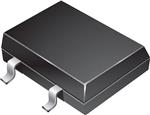
- 引脚数量:4个引脚
- 封装:SMT封装,直接安装在FR4印刷电路板上。
### 参数特性
- 最大重复峰值反向电压(VRRM):200V至800V不等,具体取决于型号。
- 最大RMS电压(VRMS):140V至560V不等。
- 最大直流阻断电压(VDC):200V至800V不等。
- 最大平均正向整流电流(I(AV)):0.8A。
- 最大直流反向电流(IR):25°C时和100°C时的值不同,具体取决于型号。
- 最大正向电压(VF):0.4A时的值为1.15V。
- 12t熔断额定值:3.7A²s。
- 最大恢复时间(TRR):150ns至500ns不等。
- 典型热阻(RθJA):50°C/W。
- 典型每个元件的结电容(CJ):13pF。
### 功能详解
- 桥式整流:提供0.8A的整流能力,可选择从200V到800V的重复峰值反向电压。
- 应用领域:家电、办公设备、电信、工厂自动化。
### 应用信息
- 应用领域:开关电源、家电、办公设备、电信、工厂自动化。
### 封装信息
- 封装类型:表面贴装封装。
- 重量:约0.125g。
- 尺寸:5mm x 7mm。
- 包装:12mm x 8mm的带卷格式,符合EIA-481标准。