Features
Applications
■ Lead free as standard**
■ Computer notebooks
■ ESD protection 30 kV max.
■ Cellular phones
■ Surge protection >24 A
■ Personal Digital Assistants (PDAs)
■ Protects 1 line
■ Digital cameras
■ Uni/bidirectional configuration
CDSOD323-TxxSC - TVS Diode Series
General Information
Additional Information
Portable communications, computing and video
equipment manufacturers are challenging the
semiconductor industry to develop increasingly smaller
electronic components.
UNIDIRECTIONAL
1
Click these links for more information:
BIDIRECTIONAL
1
PRODUCT TECHNICAL INVENTORY SAMPLES
SELECTOR LIBRARY
Bourns offers Transient Voltage Suppressor Diodes
for surge and ESD protection applications in SOD323
package size format. The Transient Voltage Suppressor
series offers a choice of voltage types ranging from 3 V
to 36 V in a unidirectional or bidirectional configuration.
2
CONTACT
2
Bourns® Chip Diodes conform to JEDEC standards, are
easy to handle on standard pick and place equipment and their flat configuration minimizes
roll away. The Bourns® device meets IEC 61000-4-2 (ESD), IEC 61000-4-4 (EFT) and IEC
61000-4-5 (Surge) requirements.
Electrical & Thermal Characteristics (@ TA = 25 °C Unless Otherwise Noted)
Parameter
Symbol
Value
Unit
Unidirectional Peak Pulse Power (tp = 8/20 μs)
PPP
500
W
Bidirectional Peak Pulse Power (tp = 8/20 μs)
PPP
400
W
TL
-55 to +150
ºC
TSTG
-55 to +150
ºC
ESD
±8
±30
±15
±30
Operating Temperature
Storage Temperature
ESD Protection (per IEC 61000-4-2)
Contact - Min.
Contact - Max.
Air - Min.
Air - Max.
kV
CDSOD323Symbol
UniT03S
BiT03SC
UniT05S
BiT05SC
UniT08S
BiT08SC
UniT12S
BiT12SC
Unit
Min. Breakdown Voltage @ 1 mA
VBR
4.0
4.0
6.0
6.0
8.5
8.5
13.3
13.3
V
Working Peak Voltage
VM
3.3
3.3
5.0
5.0
8.0
8.0
12.0
12.0
V
Maximum Clamping Voltage @ IP = 1 A
VF
7.0
8.0
9.8
9.8
13.4
13.4
19.0
19.0
V
VC
10.9 V
@ 43 A
10.9
V@
43 A
13.5
V@
42 A
14.5
V@
28 A
16.9
V@
34 A
18.5 V
@ 17
A
25.9 V
@ 21 A
29.5 V
@ 14 A
V
Maximum Leakage Current @ VWM
ID
125
125
10
10
10
10
1
1
μA
Typical Capacitance @ 0 V, 1 MHz
CP
500
200
350
175
250
150
150
50
pF
Parameter
Typical Clamping Voltage
@ 8/20 μs @ IPP
Notes:
1. Part numbers with suffix “C” indicate bidirectional device, i.e. CDSOD323-T05SC.
2. For bidirectional devices only, the electrical specifications apply in both directions.
WARNING Cancer and Reproductive Harm - www.P65Warnings.ca.gov
*RoHS Directive 2015/863, Mar 31, 2015 and Annex.
**No lead detected in standard tests of homogeneous materials.
Specifications are subject to change without notice.
Users should verify actual device performance in their specific applications.
The products described herein and this document are subject to specific legal disclaimers as set forth on the last page of this document, and at www.bourns.com/docs/legal/disclaimer.pdf.
�CDSOD323-TxxSC - TVS Diode Series
Electrical & Thermal Characteristics (@ TA = 25 °C Unless Otherwise Noted)
CDSOD323Parameter
Symbol
UniT15S
BiT15SC
UniT18S
BiT18SC
UniT24S
BiT24SC
UniT36S
BiT36SC
Unit
Min. Breakdown Voltage @ 1 mA
VBR
16.7
16.7
20.0
20.0
26.7
26.7
40.0
40.0
V
Working Peak Voltage
VM
15.0
15.0
18.0
18.0
24.0
24.0
36.0
36.0
V
Maximum Clamping Voltage
@ IP = 1 A
VF
24.0
24.0
29.0
29.0
43.0
43.0
60.0
60.0
V
VC
30.0 V
@ 17 A
33.0 V
@ 12 A
40.0 V
@9A
40.0 V
@9A
49.0 V
@ 12 A
46.2 V
@9A
75.0 V
@5A
75.0 V
@5A
V
100
40
90
40
88
40
75
35
Typical Clamping Voltage
@ 8/20 μs @ IPP
Maximum Leakage Current @ VWM
ID
Typical Capacitance @ 0 V, 1 MHz
CP
1
μA
pF
Notes:
1. Part numbers with suffix “C” indicate bidirectional device, i.e. CDSOD323-T05SC.
2. For bidirectional devices only, the electrical specifications apply in both directions.
Performance Graphs
Peak Pulse Power vs. Pulse Time
Pulse Waveform
120
500 W, 8/20 µs Waveform
1,000
100
400 W, 8/20 µs Waveform
IPP – Peak Pulse Current (% of IPP)
PPP – Peak Pulse Current (W)
10,000
Test Waveform Parameters
tt = 8 µs
td = 20 µs
tt
100
80
et
60
40
td = t|IPP/2
20
0
10
0.1
1
10
100
1,000
10,000
0
5
10
Block Diagram
15
20
25
30
t – Time (µs)
td – Pulse Duration (µs)
How to Order
UNIDIRECTIONAL
1
BIDIRECTIONAL
1
CD SOD323 - T 05 SC
Common Code
Chip Diode
Package
• SOD323 = SOD-323 Package
Model
T = Transient Voltage Suppressor
Working Peak Reverse Voltage
05 = 5 VRWM (Volts)
2
2
Suffix
S = Standard Capacitance Unidirectional Diode
SC = Standard Capacitance Bidirectional Diode
Specifications are subject to change without notice.
Users should verify actual device performance in their specific applications.
The products described herein and this document are subject to specific legal disclaimers as set forth on the last page of this document, and at www.bourns.com/docs/legal/disclaimer.pdf.
�CDSOD323-TxxSC - TVS Diode Series
Product Dimensions
Recommended Footprint
This is a molded JEDEC SOD-323 package with lead free 100 % Sn
plating on the terminations. It weighs approximately 30 mg and has
a flammability rating of UL 94V-0.
W
C
CATHODE BAND
(FOR UNIDIRECTIONAL
PRODUCTS ONLY)
L
A
S
L
E
Dimensions (Nominal)
B
F
D
J
Dimensions
A
1.60 - 1.90
(0.063 - 0.075)
B
1.15 - 1.45
(0.045 - 0.057)
C
2.39 - 2.70
(0.094 - 0.106)
D
0.92 - 1.14
(0.036 - 0.045)
E
0.25 - 0.40
(0.010 - 0.016)
F
0.08 - 0.20
(0.003 - 0.008)
H
0.13
(0.005) MAX.
.........
J
0.30 - 0.45
(0.012 - 0.018)
DIMENSIONS:
MM
(INCHES)
H
L
0.80
(0.031)
S
1.40
(0.055)
W
0.50
(0.020)
DIMENSIONS:
MM
(INCHES)
Typical Part Marking
Each device has device marking outlined below and the
unidirectional devices have an additional Polarity Band indicating
the cathode.
CDSOD323-T03S ............................................................................. A
CDSOD323-T03SC ......................................................................... G
CDSOD323-T05S .............................................................................B
CDSOD323-T05SC ..........................................................................H
CDSOD323-T08S .............................................................................C
CDSOD323-T08SC .......................................................................... J
CDSOD323-T12S .............................................................................D
CDSOD323-T12SC ..........................................................................K
CDSOD323-T15S .............................................................................E
CDSOD323-T15SC .......................................................................... L
CDSOD323-T18S ............................................................................ O
CDSOD323-T18SC ..........................................................................N
CDSOD323-T24S ............................................................................. F
CDSOD323-T24SC ......................................................................... M
CDSOD323-T36S .............................................................................R
CDSOD323-T36SC .......................................................................... T
Environmental Specifications
Moisture Sensitivity Level ................................................................. 1
ESD Classification (HBM)...............................................................3B
Specifications are subject to change without notice.
Users should verify actual device performance in their specific applications.
The products described herein and this document are subject to specific legal disclaimers as set forth on the last page of this document, and at www.bourns.com/docs/legal/disclaimer.pdf.
�CDSOD323-TxxSC - TVS Diode Series
Packaging Information
The surface mount product is packaged in an 8 mm x 4 mm tape and reel format per EIA-481 standard.
P
0
P
1
d
T
E
Index Hole
120 °
F
D2
W
B
D1 D
P
Trailer
.......
.......
End
A
Product
Orientation
C
Device
.......
.......
10 pitches (min.)
.......
.......
Leader
.......
.......
10 pitches (min.)
Direction of Feed
Item
Symbol
SOD-323
Carrier Width
A
1.55 ± 0.10
(0.061 ± 0.004)
Carrier Length
B
2.90 ± 0.10
(0.114 ± 0.004)
Carrier Depth
C
1.35 ± 0.10
(0.053 ± 0.004)
Sprocket Hole
d
1.55 ± 0.05
(0.061 ± 0.002)
Reel Outside Diameter
D
178
(7.008)
Reel Inner Diameter
D1
80.0
...
Min.
(3.150)
Feed Hole Diameter
D2
13.0 ± 0.20
(0.512 ± 0.008)
Sprocket Hole Position
E
1.75 ± 0.10
(0.069 ± 0.004)
Punch Hole Position
F
3.50 ± 0.05
(0.138 ± 0.002)
Punch Hole Pitch
P
4.00 ± 0.10
(0.157 ± 0.004)
Sprocket Hole Pitch
P0
4.00 ± 0.10
(0.157 ± 0.004)
Embossment Center
P1
2.00 ± 0.05
(0.079 ± 0.002)
Overall Tape Thickness
T
0.20 ± 0.10
(0.008 ± 0.004)
Tape Width
W
8.00 ± 0.20
(0.315 ± 0.008)
Reel Width
W1
.
13.5
Max.
(0.531)
--
3,000
Quantity per Reel
W1
Start
DIMENSIONS:
MM
(INCHES)
Devices are packed in accordance with EIA standard
RS-481-A.
Asia-Pacific: Tel: +886-2 2562-4117
Email: asiacus@bourns.com
EMEA: Tel: +36 88 885 877
Email: eurocus@bourns.com
The Americas: Tel: +1-951 781-5500
Email: americus@bourns.com
www.bourns.com
REV. 09/19
Specifications are subject to change without notice.
Users should verify actual device performance in their specific applications.
The products described herein and this document are subject to specific
legal disclaimers as set forth on the last page of this document, and at
www.bourns.com/docs/legal/disclaimer.pdf.
�Legal Disclaimer Notice
This legal disclaimer applies to purchasers and users of Bourns® products manufactured by or on behalf of Bourns, Inc. and
P[Z�HɉSPH[LZ��JVSSLJ[P]LS`��¸)V\YUZ¹��
Unless otherwise expressly indicated in writing, Bourns® products and data sheets relating thereto are subject to change
^P[OV\[�UV[PJL���
很抱歉,暂时无法提供与“CDSOD323-T03S”相匹配的价格&库存,您可以联系我们找货
免费人工找货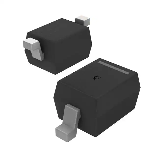


 工商网监
湘ICP备2023018690号
工商网监
湘ICP备2023018690号
