物料型号:P4SMA系列,包括不同的电压等级,如P4SMA6.8A、P4SMA7.5A等,直到P4SMA550A。
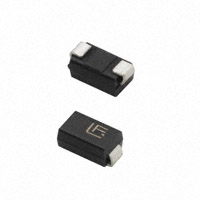
器件简介:Bourns提供的P4SMA系列瞬态电压抑制二极管,用于浪涌和ESD保护应用,采用紧凑的芯片封装DO-214AC(SMA)尺寸格式。这些器件提供从6.8V到550V的击穿电压选择,并且响应时间非常快,单向设备的典型响应时间小于1皮秒,双向设备的响应时间小于5皮秒。
引脚分配:文档中没有明确指出具体的引脚分配图,但通常SMA封装的二极管会有正负两个引脚。
参数特性:
- 峰值脉冲功率:典型值为400瓦特。
- 峰值正向浪涌电流:40安培。
- 工作温度范围:-55°C至+150°C。
- 存储温度范围:-55°C至+150°C。
功能详解:瞬态电压抑制二极管用于保护电子设备免受电压浪涌和静电放电的损害。它们具有快速响应时间,能够在皮秒级别内限制电压,从而保护敏感的电子元件。
应用信息:适用于便携式通信、计算机和视频设备等领域,这些市场对半导体行业提出了开发更小型电子元件的挑战。
封装信息:SMA(DO-214AC)封装,尺寸参数包括A、B、C、D、E、F等,具体数值请参考文档中的“Product Dimensions”部分。