Features
Applications
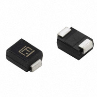
n Surface Mount SMB package
n IEC 61000-4-4 EFT
n Breakdown Voltage: 6.8 to 550 volts
n IEC 61000-4-5 Surge
n RoHS compliant* and halogen free**
n IEC 61000-4-2 ESD (Min. Level 4)
n Peak Pulse Power: 600 watts
n Typical temperature coefficient:
∆VBR = 0.1 % x VBR @ 25 °C x ∆T
P6SMB Transient Voltage Suppressor Diode Series
General Information
The markets of portable communications, computing and video equipment are challenging the semiconductor industry to develop
increasingly smaller electronic components.
Bourns offers Transient Voltage Suppressor Diodes for surge and ESD protection applications, in compact chip package DO-214AA (SMB)
size format. The Transient Voltage Suppressor series offers a choice of Breakdown Voltages from 6.8 V up to 550 V. Typical fast response
times are less than 1.0 picosecond for unidirectional devices and less than 5.0 picoseconds for bidirectional devices from 0 V to Minimum
Breakdown Voltage.
Bourns® Chip Diodes conform to JEDEC standards, are easy to handle with standard pick and place equipment and the flat configuration
minimizes roll away.
Maximum Characteristics (@ TA = 25 °C Unless Otherwise Noted)
Parameter
Peak Pulse Power Dissipation (TP = 1 ms) (Note 1,2)
Peak Forward Surge Current
8.3 ms Single Half Sine Wave Superimposed on Rated Load
(JEDEC Method) (Note 3)
Maximum Instantaneous Forward Voltage @ IPP = 50 A
(For Unidirectional Units Only)
Symbol
Value
Unit
PPK
600
Watts
IFSM
100
Amps
VF
3.5
5.0
Volts
TJ
-55 to +150
°C
-55 to +150
°C
P6SMB6.8A ~ P6SMB200A
P6SMB220A ~ P6SMB550A
Operating Temperature Range
Storage Temperature Range
TSTG
1. Non-repetitive current pulse, per Pulse Waveform graph and derated above TA = 25 °C per Pulse Derating Curve.
2. Thermal Resistance Junction to Lead.
3. 8.3 ms Single Half-Sine Wave duty cycle = 4 pulses maximum per minute (unidirectional units only).
How to Order
Asia-Pacific:
Tel: +886-2 2562-4117
Email: asiacus@bourns.com
Europe:
Tel: +36 88 885 877
Email: eurocus@bourns.com
The Americas:
Tel: +1-951 781-5500
Email: americus@bourns.com
www.bourns.com
P6SMB 6.8 CA - H
Series
P6SMB= SMB/DO-214AA
Breakdown Voltage
6.8 to 550 = 6.8 to 550 VBD (Volts)
Suffix
A = 5 % Tolerance Unidirectional Device
CA = 5 % Tolerance Bidirectional Device
Reel
(blank) = 13 inch reel
-H = 7 inch reel
* RoHS Directive 2015/863, Mar 31, 2015 and Annex.
**Bourns considers a product to be “halogen free” if (a) the Bromine (Br) content is 900 ppm or less; (b) the Chlorine (Cl) content is 900 ppm or less; and (c) the total Bromine (Br)
and Chlorine (Cl) content is 1500 ppm or less.
Specifications are subject to change without notice.
Users should verify actual device performance in their specific applications.
The products described herein and this document are subject to specific legal disclaimers as set forth on the last page of this document, and at www.bourns.com/docs/legal/disclaimer.pdf.
�
P6SMB Transient Voltage Suppressor Diode Series
Electrical Characteristics (@ TA = 25 °C Unless Otherwise Noted)
Unidirectional Device
Bidirectional Device
Breakdown Voltage
VBR (Volts)
Part No.
Marking
Part No.
Marking
Min.
Max.
P6SMB6.8A
P6SMB7.5A
P6SMB8.2A
P6SMB9.1A
P6SMB10A
P6SMB11A
P6SMB12A
P6SMB13A
P6SMB15A
P6SMB16A
P6SMB18A
P6SMB20A
P6SMB22A
P6SMB24A
P6SMB27A
P6SMB30A
P6SMB33A
P6SMB36A
P6SMB39A
P6SMB43A
P6SMB47A
P6SMB51A
P6SMB56A
P6SMB62A
P6SMB68A
P6SMB75A
P6SMB82A
P6SMB91A
P6SMB100A
P6SMB110A
P6SMB120A
P6SMB130A
P6SMB150A
P6SMB160A
P6SMB170A
P6SMB180A
P6SMB200A
P6SMB220A
P6SMB250A
P6SMB300A
P6SMB350A
P6SMB400A
P6SMB440A
P6SMB480A
P6SMB510A
P6SMB530A
P6SMB540A
P6SMB550A
6V8A
7V5A
8V2A
9V1A
10A
11A
12A
13A
15A
16A
18A
20A
22A
24A
27A
30A
33A
36A
39A
43A
47A
51A
56A
62A
68A
75A
82A
91A
100A
110A
120A
130A
150A
160A
170A
180A
200A
220A
250A
300A
350A
400A
440A
480A
510A
530A
540A
550A
P6SMB6.8CA
P6SMB7.5CA
P6SMB8.2CA
P6SMB9.1CA
P6SMB10CA
P6SMB11CA
P6SMB12CA
P6SMB13CA
P6SMB15CA
P6SMB16CA
P6SMB18CA
P6SMB20CA
P6SMB22CA
P6SMB24CA
P6SMB27CA
P6SMB30CA
P6SMB33CA
P6SMB36CA
P6SMB39CA
P6SMB43CA
P6SMB47CA
P6SMB51CA
P6SMB56CA
P6SMB62CA
P6SMB68CA
P6SMB75CA
P6SMB82CA
P6SMB91CA
P6SMB100CA
P6SMB110CA
P6SMB120CA
P6SMB130CA
P6SMB150CA
P6SMB160CA
P6SMB170CA
P6SMB180CA
P6SMB200CA
P6SMB220CA
P6SMB250CA
P6SMB300CA
P6SMB350CA
P6SMB400CA
P6SMB440CA
P6SMB480CA
P6SMB510CA
P6SMB530CA
P6SMB540CA
P6SMB550CA
6V8C
7V5C
8V2C
9V1C
10C
11C
12C
13C
15C
16C
18C
20C
22C
24C
27C
30C
33C
36C
39C
43C
47C
51C
56C
62C
68C
75C
82C
91C
100C
110C
120C
130C
150C
160C
170C
180C
200C
220C
250C
300C
350C
400C
440C
480C
510C
530C
540C
550C
6.45
7.13
7.79
8.65
9.5
10.5
11.4
12.4
14.3
15.2
17.1
19
20.9
22.8
25.7
28.5
31.4
34.2
37.1
40.9
44.7
48.5
53.2
58.9
64.6
71.3
77.9
86.5
95
105
114
124
143
152
162
171
190
209
237
285
332
380
418
456
485
503.5
513
522.5
7.14
7.88
8.61
9.55
10.5
11.6
12.6
13.7
15.8
16.8
18.9
21
23.1
25.2
28.4
31.5
34.7
37.8
41
45.2
49.4
53.6
58.8
65.1
71.4
78.8
86.1
95.5
105
116
126
137
158
168
179
189
210
231
263
315
368
420
462
504
535
556.5
567
577.5
@ IT
(mA)
10
10
10
1
1
1
1
1
1
1
1
1
1
1
1
1
1
1
1
1
1
1
1
1
1
1
1
1
1
1
1
1
1
1
1
1
1
1
1
1
1
1
1
1
1
1
1
1
Working
Peak
Reverse
Voltage
Maximum
Reverse
Leakage
@ VRWM
VRWM
(V)
IR
(μA)
5.8
6.4
7.02
7.78
8.55
9.4
10.2
11.1
12.8
13.6
15.3
17.1
18.8
20.5
23.1
25.6
28.2
30.8
33.3
36.8
40.2
43.6
47.8
53
58.1
64.1
70.1
77.8
85.5
94
102
111
128
136
145
154
171
185
214
256
300
342
376
408
434
477
486
495
1000
500
200
50
10
5
5
1
1
1
1
1
1
1
1
1
1
1
1
1
1
1
1
1
1
1
1
1
1
1
1
1
1
1
1
1
1
1
1
1
1
1
1
1
1
1
1
1
Maximum
Clamping
Voltage
@ Ipp
Maximum
Peak
Pulse
Current
Maximum
Clamping
Voltage
@ Ipp
Maximum
Peak
Pulse
Current
Vc
(V)
Ipp
(A)
Vc
(V)
Ipp
(A)
(10/1000 µs)
10.5
11.3
12.1
13.4
14.5
15.6
16.7
18.2
21.2
22.5
25.5
27.7
30.6
33.2
37.5
41.4
45.7
49.9
53.9
59.3
64.8
70.1
77
85
92
103
113
125
137
152
165
179
207
219
234
246
274
328
344
414
482
548
602
658
698
725
740
760
(10/1000 µs)
58.1
54
50.4
45.5
42.1
39.1
36.5
33.5
28.8
27.1
24.2
22
19.9
18.4
16.3
14.7
13.3
12.2
11.3
10.3
9.4
8.7
7.9
7.2
6.6
5.9
5.4
4.9
4.5
4
3.7
3.4
2.9
2.8
2.6
2.5
2.2
1.9
1.8
1.5
1.3
1.1
1
0.9
0.9
0.8
0.8
0.8
(8/20 µs)
13.7
15
15.7
17.4
18.9
20.3
21.7
23.7
27.6
29.3
33.2
36
39.8
43.2
48.8
53.8
59.4
64.9
70.1
77.1
84.2
91.1
100.1
110.5
119.6
133.9
146.9
162.5
178.1
198
214.5
232.7
269.1
284.7
304.2
319.8
356.2
426.4
447.2
538.2
626.6
712.4
783
855.4
907.4
942.5
962.0
988.0
(8/20 µs)
290.5
270
252.0
227.5
210.5
195.5
182.5
167.5
144.0
135.5
121.0
110
99.5
92.0
81.5
73.5
66.5
61.0
56.5
51.5
47.0
43.5
39.5
36.0
33.0
29.5
27.0
24.5
22.5
20
18.5
17.0
14.5
14.0
13.0
12.5
11.0
9.5
9.0
7.5
6.5
5.5
5
4.6
4.3
4.1
4.1
3.9
Notes:
1. Suffix ‘A’ denotes a 5 % tolerance unidirectional device.
2. Suffix ‘CA’ denotes a 5 % tolerance bidirectional device.
3. For bidirectional devices with a VR of 10 volts or less, the IR limit is double.
Specifications are subject to change without notice.
Users should verify actual device performance in their specific applications.
The products described herein and this document are subject to specific legal disclaimers as set forth on the last page of this document, and at www.bourns.com/docs/legal/disclaimer.pdf.
�P6SMB
Voltage
Suppressor
Diode Series
3312
- 2Transient
mm SMD
Trimming
Potentiometer
Rating & Characteristic Curves
Peak Pulse Derating in Percent of
Peak Pulse Derating in Percent of
Peak Pulse Derating in Percent of
Peak Power or Current
Peak Power or Current
Peak Pulse Derating in Percent of
Peak Power or Current
Peak Power or Current
Peak Pulse Derating in Percent of
Peak Pulse Derating in Percent of
Peak Power or Current
Peak Power or Current
100100
75
75
120
100120 100
100
100
75
75
100
80100 80
80
80
75 75
50
50
80
60 80 60
60
60
50
50
50 50
25
25
Peak Forward Surge Current (Amps)
Peak Forward Surge Current (Amps)
Maximum
120 120
120 Non-Repetitive Surge Current
120
Peak Forward Surge Current (Amps)
Peak Forward Surge Current (Amps)
Peak Forward Surge Current (Amps)
Peak Forward Surge Current (Amps)
Pulse 100
Derating
100 100
100 Curve
60
40 60 40
40
40
25
25
Pulse Width 8.3 ms
Pulse Width 8.3 ms
Pulse Width 8.3 ms
Pulse Width 8.3 ms
20 Single Half Sine-Wave
20
Single Half Sine-Wave
Single Half Sine-Wave
Single Half Sine-Wave
Pulse Width 8.3 ms
Pulse Width 8.3 ms
200 20 0 Single Half Sine-Wave
Single Half Sine-Wave
0
0
10
10
20
20 50
50
50 100
100 100
100
11
20
1212
22 55
55 10
10
20
50
0 0
Number of Cycles at 60 Hz
Number of Cycles at 60 Hz
Number of Cycles at 60 Hz
Number of Cycles at 60 Hz
1 1 2 2
5 5
10 10 20 20
50 50
100100
40
20
20
25 25
00
00
25
25
50
75
50 100
100
75 100
100
125 125
125
150 150
150
175 175
175
200 200
200
00
50
75
125
150
175
200
0025
25
50
75
0 0
°C)
°C)
Ambient Temperature (
Ambient Temperature (
°C)
Ambient Temperature (
°C)
Ambient Temperature (
0 0 25 25 50 50 75 75 100100 125125 150150 175175 200200
40
Number of Cycles at 60 Hz
Number of Cycles at 60 Hz
Ambient Temperature (
Ambient Temperature (
°C) °C)
Pulse Waveform
Typical Junction Capacitance
10000 10000
10000
10000
1.0
1.0
1.0 1.0
1.0 2.0
2.0
1.0
2.0
2.0
3.0
3.0
3.0
3.0
T, Time (ms)
T, Time (ms)3.0
T, Time (ms)
2.0 2.0T, Time (ms)
3.0
4.0
4.0
CCJ Junction Capacitance (pF)
J - Junction Capacitance (pF)
CCJ - Junction Capacitance (pF)
CJ - Junction Capacitance (pF)
J - Junction Capacitance (pF)
CJ - Junction Capacitance (pF)
00
00
00
00
0 0
0 0
100
100
4.0
4.0
4.0 4.0
1.0 1.0
1.0
1.0
10
10
= 25 ° C
= 25 ° C
TT = 25 ° C
10 10TT = 25 ° C
f = 1.0 MHz
f = 1.0 MHz
f = 1.0 MHz
f = 1.0 MHz
T = 25 ° C
Vsig = 50 mVp-p
TVsig = 50 mVp-p
= 25 ° C
Vsig = 50 mVp-p
Vsig = 50 mVp-p
11 f = 1.0 MHz
11f = 1.0 MHz
Vsig = 50 mVp-p
1
10
11 Vsig = 50 mVp-p
10
1 1
1 1
5.0
5.0
TA = 25 °C
TA = 25 °C
Non-repetitive
Non-repetitive
Non-repetitive
Non-repetitive
Pulse Waveform
Pulse Waveform
Pulse Waveform
Pulse Waveform
Non-repetitive
Non-repetitive
Shown in Pulse Waveform Graph
Shown in Pulse Waveform Graph
Shown in Pulse Waveform Graph
Shown in Pulse Waveform Graph
Pulse Waveform
Pulse Waveform
Shown in Pulse Waveform Graph
Shown in Pulse Waveform Graph
RM(AV) Steady State Power Dissipation (W)
RM(AV) Steady State Power Dissipation (W)
1.0
1.0
10
10
1
Bidirectional @VR
Bidirectional @VR
Bidirectional @VR
Bidirectional @VR
10
10
Bidirectional @VR
Bidirectional @VR
100
100
100
100
1000 1000
1000
1000
10
1000
- Reverse Breakdown Voltage (V)
- Reverse Breakdown Voltage (V)
10 - Reverse Breakdown Voltage (V)
100100
1000
VVBR
VVBR
BR
BR - Reverse Breakdown Voltage (V)
V V - Reverse Breakdown Voltage (V)
BR - Reverse Breakdown Voltage (V)
TA = 25 °C
TA = 25 °C
TA = 25 °C
TA = 25 °C
10 10
100 Unidirectional @VR
100
Unidirectional @VR
Steady State PowerBRDerating Curve
100
100
10
10
Unidirectional @VR
Unidirectional @VR
Unidirectional @VR
Unidirectional @VR
100100
RM(AV) Steady State Power Dissipation (W)
RM(AV) Steady State Power Dissipation (W)
RM(AV) Steady State Power Dissipation (W)
RM(AV) Steady State Power Dissipation (W)
PPPP, Peak Power (KW)
, Peak Power (KW)
10
10
Bidirectional V = 0 V
Bidirectional V = 0 V
10001000
Pulse Rating Curve
100100
Unidirectional V = 0 V
Unidirectional V = 0 V
Bidirectional V = 0 V
Bidirectional V = 0 V
Bidirectional V = 0 V
Bidirectional V = 0 V
1000 1000
1000
1000
T, Time (ms)
T, Time (ms)
100
100
Unidirectional V = 0 V
Unidirectional V = 0 V
Unidirectional V = 0 V
Unidirectional V = 0 V
10000
10000
IIPP, Peak Pulse Current (%)
, Peak Pulse Current (%)
IIP, Peak Pulse Current (%)
IP, Peak Pulse Current (%)
P, Peak Pulse Current (%)
IP, Peak Pulse Current (%)
TR=10 µs
TR=10 µs
TR=10 µs
TR=10 µs
Peak value (IRSM)
Peak value (IRSM)
Peak value (IRSM)
Peak value (IRSM)
100 100
100 TR=10 µs
TR=10 µs
100
IRSM IRSM
IRSM
IRSM
Peak value (IRSM)
Half value=
Half value=
Peak value (IRSM)
Half value=
Half value=
100100
22
22
IRSM
IRSM
Half value=
Half value=
2
Pulse width (TP)
Pulse width (TP)
2
Pulse width (TP)
Pulse width (TP)
is defined as that point
is defined as that point
is defined as that point
is defined as that point
where the peak current
where the peak current
where the peak current
Pulse width (TP)
where the peak current
Pulse width (TP)
decays to 50 % of IPSM.
decays to 50 % of IPSM.
decays to 50 % of IPSM.
is defined as that point
decays to 50 % of IPSM.
50
50
is defined as that point
50
50
where the peak current
where the peak current
10 x 1000 waveform
10 x 1000 waveform
10 x 1000 waveform
decays to 50 % of IPSM.
10 x 1000 waveform
decays to 50 % of IPSM.
50 50 TA=25 °C
TA=25 °C
TA=25 °C
as defined by R.E.A.
as defined by R.E.A.
TA=25 °C
as defined by R.E.A.
as defined by R.E.A.
TP
TP
10 x 1000 waveform
TP
TP
10 x 1000 waveform
TA=25 °C
as defined by R.E.A.
TA=25 °C
as defined by R.E.A.
TP TP
PPP, Peak Power (KW)
PP, Peak Power (KW)
P, Peak Power (KW)
PP, Peak Power (KW)
5.0
5.0
5.0 5.0
4.0
4.0
4.0
4.0
4.0 4.0
3.0 3.0
3.0
3.0
3.0 3.0
2.0 2.0
2.0
2.0
2.0 2.0
1.0 1.0
1.0
1.0
1.0 1.0
60 Hz Resistive or
60 Hz Resistive or
60 Hz Resistive or
60 Hz Resistive or
Inductive Load
Inductive Load
Inductive Load
Inductive Load
60 Hz Resistive or
60 Hz Resistive or
Inductive Load
25
50 Inductive Load
50
75
75
100 100
100
125
50
75
100
125
50
25
75
0.0 0.0
0.0
0.1
0.1 0.1
0.0
0.1
25
125
150 150
150
175 175
175
200 200
200
1.0 µs 1.0 µs
10 µs 10 µs
100 µs100 µs
100 µs
1.0 ms1.0 ms
1.0 ms
10 ms 10 ms
0.1 µs
1.0 µs
10 µs100 µs
10 ms
0.1 µs 0.1 µs
00
150
175
200
1.0 ms
0.1 µs
1.0 µs
10 µs
10 ms
00 25
125
0.0 0.0
0.1 0.1
TL, Lead Temperature (°C)
TL, Lead Temperature (°C)
TP, Pulse Width
TP, Pulse Width
TL, Lead Temperature (°C)
TP, Pulse Width
TL, Lead Temperature (°C)
TP, Pulse Width
0.1 µs 1.0 µs
1.0 µs 10 µs
10 µs 100 µs
10 ms
100 µs 1.0 ms
1.0 ms 10 ms
0 0
25 25 50 50 75 75 100100 125125 150150 175175 200200
0.1 µs
Specifications are subject to change without notice.
TL, Lead Temperature (°C)
TP, Pulse Width
TL, Lead Temperature (°C)
TP, Pulse Width
Users should verify actual device performance in their specific applications.
The products described herein and this document are subject to specific legal disclaimers as set forth on the last page of this document, and at www.bourns.com/docs/legal/disclaimer.pdf.
� P6SMB
Voltage
Suppressor
Diode Series
3312Transient
- 2 mm SMD
Trimming
Potentiometer
Product Dimensions
Recommended Footprint
CATHODE
BAND
A
a
A
A
(FOR UNIDIRECTIONAL
PRODUCTS ONLY)
B
C
B
b
B
c
C
F
D
G
Dimension
A
B
C
D
E
F
G
a (Max.)
E
C
D
DIMENSIONS:
b (Min.)
MM
(INCHES)
SMB (DO-214AA)
4.06 - 4.57
(0.160 - 0.180)
3.30 - 3.94
E
(0.130 - 0.155)
1.95 - 2.20
(0.077 - 0.087)
MM
DIMENSIONS:
(INCHES)
5.21 - 5.59
(0.205 - 0.220)
0.05 - 0.203
(0.002 - 0.008)
2.13 - 2.44
(0.084 - 0.096)
0.76 - 1.52
(0.030 - 0.060)
DIMENSIONS:
Dimension
F
c (Min.)
SMB (DO-214AA)
2.69
(0.106)
2.10
(0.083)
1.27
(0.050)
DIMENSIONS:
MM
(INCHES)
Physical Specifications
Case............................................Molded plastic per UL Class 94V-0
Polarity....................... Cathode band indicates unidirectional device
No cathode band indicates bidirectional device
Environmental Specifications
Moisture Sensitivity Level.................................................................1
ESD Classification (HBM)............................................................. 3B
MM
(INCHES)
Specifications are subject to change without notice.
Users should verify actual device performance in their specific applications.
The products described herein and this document are subject to specific legal disclaimers as set forth on the last page of this document, and at www.bourns.com/docs/legal/disclaimer.pdf.
�
P6SMB Transient- TVS/Steering
Voltage Suppressor
Diode Series
CDDFN5-0504N
Diode Array
Packaging Information
The product will be dispensed in tape and reel format (see diagram below).
P
0
P
1
d
T
E
Index Hole
120 °
F
D2
W
B
D1 D
P
Trailer
.......
.......
End
A
Unidirectional
Product
Orientation
C
Device
.......
.......
.......
.......
Leader
.......
.......
10 pitches (min.)
W1
Start
DIMENSIONS:
MM
(INCHES)
10 pitches (min.)
Direction of Feed
Item
Symbol
Carrier Width
A
Carrier Length
B
Carrier Depth
C
Sprocket Hole
d
Reel Outside Diameter
D
Reel Inner Diameter
D1
Feed Hole Diameter
D2
Sprocket Hole Position
E
Punch Hole Position
F
Punch Hole Pitch
P
Sprocket Hole Pitch
P0
Embossment Center
P1
Overall Tape Thickness
T
Tape Width
W
Reel Width
W1
Quantity per Reel
--
Devices are packed in accordance with EIA standard
RS-481-A and specifications shown here.
SMB (DO-214AA)
7 Inch Reel
13 Inch Reel
3.67 ± 0.20
(0.144 ± 0.008)
5.60 ± 0.20
(0.220 ± 0.008)
2.57 ± 0.20
(0.101 ± 0.008)
1.50 ± 0.10
(0.059 ± 0.004)
178
330
(7.008)
(12.992)
50.0
MIN.
(1.969)
13.0 ± 0.20
(0.512 ± 0.008)
1.75 ± 0.10
(0.069 ± 0.004)
5.50 ± 0.05
(0.217 ± 0.002)
8.00 ± 0.10
(0.315 ± 0.004)
4.00 ± 0.10
(0.157 ± 0.004)
2.00 ± 0.05
(0.079 ± 0.002)
0.30 ± 0.10
(0.012 ± 0.004)
12.00 ± 0.30
(0.472 ± 0.012)
18.4
MAX.
(0.724)
500
3,000
REV. 03/20
Specifications are subject to change without notice.
Users should verify actual device performance in their specific applications.
The products described herein and this document are subject to specific legal disclaimers as set forth on the last page of this document, and at www.bourns.com/docs/legal/disclaimer.pdf.
�
Legal Disclaimer Notice
This legal disclaimer applies to purchasers and users of Bourns® products manufactured by or on behalf of Bourns, Inc. and its
affiliates (collectively, “Bourns”).
Unless otherwise expressly indicated in writing, Bourns® products and data sheets relating thereto are subject to change
without notice. Users should check for and obtain the latest relevant information and verify that such information is current and
complete before placing orders for Bourns® products.
The characteristics and parameters of a Bourns® product set forth in its data sheet are based on laboratory conditions, and
statements regarding the suitability of products for certain types of applications are based on Bourns’ knowledge of typical
requirements in generic applications. The characteristics and parameters of a Bourns® product in a user application may vary
from the data sheet characteristics and parameters due to (i) the combination of the Bourns® product with other components
in the user’s application, or (ii) the environment of the user application itself. The characteristics and parameters of a Bourns®
product also can and do vary in different applications and actual performance may vary over time. Users should always verify
the actual performance of the Bourns® product in their specific devices and applications, and make their own independent
judgments regarding the amount of additional test margin to design into their device or application to compensate for
differences between laboratory and real world conditions.
Unless Bourns has explicitly designated an individual Bourns® product as meeting the requirements of a particular industry
standard (e.g., ISO/TS 16949) or a particular qualification (e.g., UL listed or recognized), Bourns is not responsible for any
failure of an individual Bourns® product to meet the requirements of such industry standard or particular qualification. Users of
Bourns® products are responsible for ensuring compliance with safety-related requirements and standards applicable to their
devices or applications.
Bourns® products are not recommended, authorized or intended for use in nuclear, lifesaving, life-critical or life-sustaining applications, nor in any other applications where failure or malfunction may result in personal injury, death, or severe property or
environmental damage. Unless expressly and specifically approved in writing by two authorized Bourns representatives on a
case-by-case basis, use of any Bourns® products in such unauthorized applications might not be safe and thus is at the user’s
sole risk. Life-critical applications include devices identified by the U.S. Food and Drug Administration as Class III devices and
generally equivalent classifications outside of the United States.
Bourns expressly identifies those Bourns® standard products that are suitable for use in automotive applications on such
products’ data sheets in the section entitled “Applications.” Unless expressly and specifically approved in writing by two
authorized Bourns representatives on a case-by-case basis, use of any other Bourns® standard products in an automotive
application might not be safe and thus is not recommended, authorized or intended and is at the user’s sole risk. If Bourns
expressly identifies a sub-category of automotive application in the data sheet for its standard products (such as infotainment
or lighting), such identification means that Bourns has reviewed its standard product and has determined that if such Bourns®
standard product is considered for potential use in automotive applications, it should only be used in such sub-category of
automotive applications. Any reference to Bourns® standard product in the data sheet as compliant with the AEC-Q standard
or “automotive grade” does not by itself mean that Bourns has approved such product for use in an automotive application.
Bourns® standard products are not tested to comply with United States Federal Aviation Administration standards generally
or any other generally equivalent governmental organization standard applicable to products designed or manufactured for
use in aircraft or space applications. Bourns expressly identifies Bourns® standard products that are suitable for use in aircraft
or space applications on such products’ data sheets in the section entitled “Applications.” Unless expressly and specifically
approved in writing by two authorized Bourns representatives on a case-by-case basis, use of any other Bourns® standard
product in an aircraft or space application might not be safe and thus is not recommended, authorized or intended and is at the
user’s sole risk.
The use and level of testing applicable to Bourns® custom products shall be negotiated on a case-by-case basis by Bourns and
the user for which such Bourns® custom products are specially designed. Absent a written agreement between Bourns and the
user regarding the use and level of such testing, the above provisions applicable to Bourns® standard products shall also apply
to such Bourns® custom products.
Users shall not sell, transfer, export or re-export any Bourns® products or technology for use in activities which involve the
design, development, production, use or stockpiling of nuclear, chemical or biological weapons or missiles, nor shall they use
Bourns® products or technology in any facility which engages in activities relating to such devices. The foregoing restrictions
apply to all uses and applications that violate national or international prohibitions, including embargos or international
regulations. Further, Bourns® products and Bourns technology and technical data may not under any circumstance be
exported or re-exported to countries subject to international sanctions or embargoes. Bourns® products may not, without prior
authorization from Bourns and/or the U.S. Government, be resold, transferred, or re-exported to any party not eligible
to receive U.S. commodities, software, and technical data.
To the maximum extent permitted by applicable law, Bourns disclaims (i) any and all liability for special, punitive, consequential,
incidental or indirect damages or lost revenues or lost profits, and (ii) any and all implied warranties, including implied warranties
of fitness for particular purpose, non-infringement and merchantability.
For your convenience, copies of this Legal Disclaimer Notice with German, Spanish, Japanese, Traditional Chinese and Simplified Chinese
bilingual versions are available at:
Web Page: http://www.bourns.com/legal/disclaimers-terms-and-policies
PDF: http://www.bourns.com/docs/Legal/disclaimer.pdf
C1753 05/17/18R
�


 工商网监
湘ICP备2023018690号
工商网监
湘ICP备2023018690号
