Features
■ Formerly a
product
■ Two model sizes available - 3255 & 4032
PV
40 300
32 K
■ Operating voltage range (Vdc) 14 V to 385 V
■ Operating voltage (Vrms) 11 V to 300 V
■ Easily solderable tinned copper sheet
■ Available in tape and reel packaging for
automatic pick-and-place
■ RoHS compliant*
■ +85 °C Continuous operating temperature
■ UL 94 V-0 Non-flammable thermoplastic
encapsulation
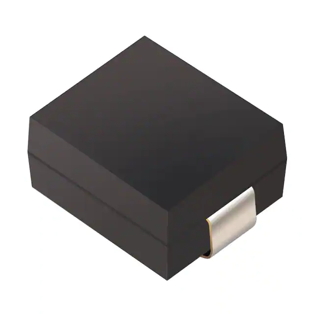
PV Series - Low & Medium Voltage Plastic-Encapsulated Varistors
General Information
Additional Information
The PV series of low and medium voltage plastic-encapsulated varistors is designed
to protect electronic equipment against voltage surges in the low and medium voltage
region. They offer direct SMD equivalents to leaded disc varistors of 5 and 7 mm sizes.
The thermoplastic encapsulation is non-flammable and UL 94 V-0 rated. Contacts are
made of tinned copper sheet.
PV series varistors are designed for surface mounting and are available in two model
sizes.
These transient voltage suppressors cover an operating voltage Vrms from 11 V to
300 V, featuring maximum surge currents from 100 A to 1200 A.
Absolute Maximum Ratings
Parameter
Continuous:
Steady State Applied Voltage
DC Voltage Range (Vdc)
AC Voltage Range (Vrms)
Transient:
Non-Repetitive Surge Current, 8/20 μs Waveform (Imax)
Non-Repetitive Surge Energy, 10/1000 μs Waveform (Wmax)
Operating Ambient Temperature
Storage Temperature Range
Threshold Voltage Temperature Coefficient
Response Time
Climatic Category
Value
Units
14 to 385
11 to 300***
V
V
100 to 1200
0.6 to 30
-40 to +85
-40 to +125
< +0.05
(.472)
B0
P1 ± 0.1
(P1 ± .004)
F ± 0.05
(F ± .002)
20 ° MAX: W =
Reel
2 ± 0.5
(.079 ± .020)
21 ± 0.8
(.827 ± .315)
12.80 + 0.5
(.504 + .020)
W1
A - 2.0
(A - 0.79)
60 + 2.0
(2.362 + .079)
PV 11 K 3225 ~ PV 150 K 3225 =
1,500 pieces per 13-inch reel
All other models =
1,000 pieces per 13-inch reel
W2
Model Size
Dimension
Size
A0
B0
K0 MAX.
B1 MAX.
D1 DIA. MAX.
e2
Model Size
Dimension
3225
4032
7
(.276)
7.8
(.307)
8.6
(.339)
10.8
(.425)
3225
P1
F
3.7
(.146)
12.1
(.476)
1.5
(.059)
14.25
(.561)
12
(.472)
W
T2 MAX.
W1
W2 MAX.
A DIA.
DIMENSIONS:
4032
7.5
(.295)
16.0
(.630)
9.5
(.374)
16.4 + 2
(.646 + .079)
22.4
(.882)
15.9
19.4
to
(.626) (.764)
330
(12.992)
MM
(INCHES)
Specifications are subject to change without notice.
Users should verify actual device performance in their specific applications.
The products described herein and this document are subject to specific legal disclaimers as set forth on the last page of this document, and at www.bourns.com/docs/legal/disclaimer.pdf.
�PV Series - Low & Medium Voltage Plastic-Encapsulated Varistors
Soldering Recommendations for SMD Components
Popular soldering techniques used for surface mounted components are Wave and Infrared Reflow processes. Both processes can be
performed with Pb-containing or Pb-free solders. The termination options available for these soldering techniques are AgPd and Barrier
Type End Terminations.
End Termination
Ag/Pd
Barrier Type End Termination
NiSn End Termination
Designation
Recommended and Suitable for
RoHS Compliant
PV Series…R1
PV Series…N R1
PV Series ...Ni R1
Pb-containing soldering
Pb-containing and Pb-free soldering
Pb-containing and Pb-free soldering
Yes
Yes
Yes
Wave Soldering
This process is generally associated with discrete components mounted on the underside of printed circuit boards, or for large top-side
components with bottom-side mounting tabs to be attached, such as the frames of transformers, relays, connectors, etc. SMD varistors
to be wave soldered are first glued to the circuit board, usually with an epoxy adhesive. When all components on the PCB have been
positioned and an appropriate amount of time is allowed for adhesive curing, the completed assembly is then placed on a conveyor and
run through a single, double wave process.
Infrared Reflow Soldering
These reflow processes are typically associated with top-side component placement. This technique utilizes a mixture of adhesive
and solder compounds (and sometimes fluxes) that are blended into a paste. The paste is then screened onto PCB soldering pads
specifically designed to accept a particular sized SMD component. The recommended solder paste wet layer thickness is 100 to 300 μm.
Once the circuit board is fully populated with SMD components, it is placed in a reflow environment, where the paste is heated to slightly
above its eutectic temperature. When the solder paste reflows, the SMD components are attached to the solder pads.
Solder Fluxes
Solder fluxes are generally applied to populated circuit boards to keep oxides from forming during the heating process and to facilitate
the flowing of the solder. Solder fluxes can be either a part of the solder paste compound or separate materials, usually fluids.
Recommended fluxes are:
• non-activated (R) fluxes, whenever possible
• mildly activated (RMA) fluxes of class L3CN
• class ORLO
Activated (RA), water soluble or strong acidic fluxes with a chlorine content > 0.2 wt. % are NOT RECOMMENDED. The use of such
fluxes could create high leakage current paths along the body of the varistor components.
When a flux is applied prior to wave soldering, it is important to completely dry any residual flux solvents prior to the soldering process.
Thermal Shock
To avoid the possibility of generating stresses in the varistor chip due to thermal shock, a preheat stage to within 100 °C of the peak
soldering process temperature is recommended. Additionally, SMD varistors should not be subjected to a temperature gradient greater
than 4 °C/sec., with an ideal gradient being 2 °C/sec. Peak temperatures should be controlled. Wave and Reflow soldering conditions
for SMD varistors with Pb-containing solders are shown on the next page in Fig. 1 and 2 respectively, while Wave and Reflow soldering
conditions for SMD varistors with Pb-free solders are shown in Fig. 1 and 3.
Whenever several different types of SMD components are being soldered, each having a specific soldering profile, the soldering profile
with the least heat and the minimum amount of heating time is recommended. Once soldering has been completed, it is necessary to
minimize the possibility of thermal shock by allowing the hot PCB to cool to less than 50 °C before cleaning.
Specifications are subject to change without notice.
Users should verify actual device performance in their specific applications.
The products described herein and this document are subject to specific legal disclaimers as set forth on the last page of this document, and at www.bourns.com/docs/legal/disclaimer.pdf.
�PV Series - Low & Medium Voltage Plastic-Encapsulated Varistors
Soldering Recommendations for SMD Components (Continued)
Inspection Criteria
When Infrared Reflow processes are used, the inspection criteria to determine acceptable solder joints will depend on several key
variables, principally termination material process profiles.
Solder Test and Retained Samples
Reflow soldering test based on J-STD-020D.1 and soldering test by dipping based on IEC 60068- 2 for Pb-free solders are performed on
each production lot. Test results and accompanying samples are retained for a minimum of two (2) years. The solderability of a specific
lot can be checked at any time within this period, should a customer require this information.
Rework Criteria - Soldering Iron
Unless absolutely necessary, the use of soldering irons is NOT recommended for reworking varistors encapsulated in plastic. If no other
means of rework is available, the following criteria must be strictly followed:
• Do not allow the tip of the iron to directly contact the top of the plastic
• Do not exceed the following soldering iron specifications:
Output Power.......................................30 Watts Maximum
Temperature of Soldering Iron Tip .......280 °C Maximum
Soldering Time .....................................10 Seconds Maximum
Storage Conditions
SMD varistors should be used within 1 year of purchase to avoid possible soldering problems caused by oxidized terminals. The storage
environment should be controlled, with humidity less than 40 % and temperature between -25 and +45 °C. Varistor chips should always
be stored in their original packaged unit.
Specifications are subject to change without notice.
Users should verify actual device performance in their specific applications.
The products described herein and this document are subject to specific legal disclaimers as set forth on the last page of this document, and at www.bourns.com/docs/legal/disclaimer.pdf.
�PV Series - Low & Medium Voltage Plastic-Encapsulated Varistors
Reliability Testing Procedures
Varistor test procedures comply with CECC 42200, IEC 1051-1/2 (and AEC-Q200, if applicable). Test results are available upon customer
request. Special tests can be performed upon customer request.
Reliability Parameter
Test
Tested According to
CECC 42200, Test 4.20 or
IEC 1051-1, Test 4.20,
AEC-Q200 Test 8 - 1000 h at UCT
CECC 42200, Test C 2.1 or
IEC 1051-1, Test 4.5
10 pulses in the same direction at
2 pulses per minute at maximum peak current for 10 pulses
CECC 42200, Test C 2.1 or
IEC 1051-1, Test 4.5
10 pulses in the same direction at
1 pulse every 2 minutes at maximum peak current for 10
pulses
AC/DC Bias Reliability
AC/DC Life Test
Pulse Current Capability
Imax 8/20 μs
Pulse Energy Capability
Wmax 10/1000 μs
WLD Capability
WLD x 10
ISO 7637, Test pulse 5, 10 pulses at rate of 1 per minute
Vjump Capability
Vjump 5 min.
Increase of supply voltage to V ≥ Vjump for 1 minute
Climatic Sequence
Environmental and
Storage Reliability
Thermal Shock
Steady State
Damp Heat
Storage Test
CECC 42200, Test 4.16 or
IEC 1051-1, Test 4.17
a) Dry heat, 16h, UCT, Test Ba, IEC 68-2-2
b) Damp heat, cyclic, the first cycle: 55 °C, 93 % RH, 24 h,
Test Db 68-2-4
c) Cold, LCT, 2 h, Test Aa, IEC 68-2-1
d) Damp heat cyclic, remaining 5 cycles: 55 °C, 93 % RH,
24 h/cycle, Test Bd, IEC 68-2-30
CECC 42200, Test 4.12, Test Na, IEC 68-2-14,
AEC-Q200 Test 16, 5
CECC 42200, Test 4.17, Test Ca, IEC 68-2-3,
AEC-Q200 Test 6, 56 days, 40 °C, 93 % RH,
AEC-Q200 Test 7: Bias, Rh, T all at 85.
IEC 68-2-2, Test Ba, AEC-Q200 Test 3, 1000 h at maximum
storage temperature
Condition to be
Satisfied after
Testing
|δVn (1 mA)| < 10 %
|δVn (1 mA)| < 10 %
no visible damage
|δVn (1 mA)| < 10 %
no visible damage
|δVn (1 mA)| < 15 %
no visible damage
|δVn (1 mA)| < 15 %
no visible damage
|δVn (1 mA)| < 10 %
|δVn (1 mA)| < 10 %
no visible damage
|δVn (1 mA)| < 10 %
|δVn (1 mA)| < 5 %
Continued on Next Page
Specifications are subject to change without notice.
Users should verify actual device performance in their specific applications.
The products described herein and this document are subject to specific legal disclaimers as set forth on the last page of this document, and at www.bourns.com/docs/legal/disclaimer.pdf.
�PV Series - Low & Medium Voltage Plastic-Encapsulated Varistors
Reliability Testing Procedures (Continued)
Reliability Parameter
Test
Solderability
Resistance to
Soldering Heat
Mechanical Reliability
Electrical Transient
Conduction
Tested According to
CECC 42200, Test 4.10.1, Test Ta, IEC 68-2-20 solder bath
and reflow method
CECC 42200, Test 4.10.2, Test Tb, IEC 68-2-20 solder bath
nad reflow method
JIS-C-6429, App. 1, 18N for 60 sec. - same for AEC-Q200
Terminal Strength
Test 22
JIS-C-6429, App. 2, 2 mm min.
Board Flex
AEC-Q200 test 21 - Board flex: 2 mm flex min.
CECC 42200, Test 4.15, Test Fc, IEC 68-2-6,
AEC-Q200 Test 14
Frequency range 10 to 55 Hz (AEC: 10-2000 Hz)
Vibration
Amplitude 0.75 m/s2 or 98 m/s2 (AEC: 5 g for 20 minutes) Total duration 6 h (3x2 h) (AEC: 12 cycles each of 3 directions)
Waveshape - half sine
CECC 42200, Test 4.14, Test Ea, IEC 68-2-27, AEC-Q200
Test 13.
Mechanical Shock Acceleration = 490 m/s2 (AEC: MIL-STD-202-Method 213),
Pulse duration = 11 ms,
Waveshape - half sine; Number of shocks = 3x6
AEC-Q200 Test 30: Test pulses 1 to 3.
ISO-7637-1 Pulses
Also other pulses - freestyle.
Condition to be
Satisfied after
Testing
Solderable at
shipment and after
2 years of storage,
criteria: >95% must
be covered by solder
for reflow meniscus
|δVn (1 mA)| < 5 %
No visual damage
|δVn (1 mA)| < 2 %
No visible damage
|δVn (1 mA)| < 2 %
No visible damage
|δVn (1 mA)| < 10 %
No visible damage
|δVn (1 mA)| < 10 %
No visible damage
Specifications are subject to change without notice.
Users should verify actual device performance in their specific applications.
The products described herein and this document are subject to specific legal disclaimers as set forth on the last page of this document, and at www.bourns.com/docs/legal/disclaimer.pdf.
�PV Series - Low & Medium Voltage Plastic-Encapsulated Varistors
Terminology
Term
Symbol
Definition
Rated AC Voltage ......................... Vrms ..................Maximum continuous sinusoidal AC voltage (