Features
Applications
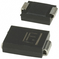
n Surface Mount SMC package
n IEC 61000-4-4 EFT
n Standoff Voltage: 5.0 to 495 volts
n IEC 61000-4-5 Surge
n RoHS compliant*
n IEC 61000-4-2 ESD (Min. Level 4)
n Power Dissipation: 1500 watts
SMCJ Transient Voltage Suppressor Diode Series
General Information
Agency Recognition
The markets of portable communications, computing and video equipment are challenging
the semiconductor industry to develop
increasingly smaller electronic components.
Description
UL
File Number: E153537
Bourns offers Transient Voltage Suppressor Diodes for surge and ESD protection
applications, in compact chip package DO-214AB (SMC) size format. The Transient Voltage
Suppressor series offers a choice of Working Peak Reverse Voltage from 5 V up to 495 V
and Breakdown Voltage up to 550 V. Typical fast response times are less than
1.0 picosecond for unidirectional devices and less than 5.0 picoseconds for bidirectional
devices from 0 V to Minimum Breakdown Voltage.
Bourns® Chip Diodes conform to JEDEC standards, are easy to handle with standard pick
and place equipment and their flat configuration minimizes roll away.
Electrical Characteristics (@ TA = 25 °C Unless Otherwise Noted)
Parameter
Minimum Peak Pulse Power Dissipation (TP = 1 ms) (Note 1,2)
Peak Forward Surge Current
8.3 ms Single Half Sine Wave Superimposed on Rated Load
(JEDEC Method) (Note 3)
Steady State Power Dissipation @ TL = 75 °C
Maximum Instantaneous Forward Voltage @ IPP = 100 A
(For Unidirectional Units Only)
Symbol
Value
Unit
PPK
1500
Watts
IFSM
200
Amps
PM(AV)
5.0
Watts
VF
3.5
5.0
Volts
TJ
-55 to +150
°C
-55 to +150
°C
SMCJ5.0A ~ SMCJ90A
SMCJ100A ~ SMCJ495A
Operating Temperature Range
Storage Temperature Range
TSTG
1. Non-repetitive current pulse, per Pulse Waveform graph and derated above TA = 25 °C per Pulse Derating Curve.
2. Thermal Resistance Junction to Lead.
3. 8.3 ms Single Half-Sine Wave duty cycle = 4 pulses maximum per minute (unidirectional units only).
How to Order
Asia-Pacific:
Tel: +886-2 2562-4117 • Email: asiacus@bourns.com
Europe:
Tel: +36 88 885 877 • Email: eurocus@bourns.com
The Americas:
Tel: +1-951 781-5500 • Email: americus@bourns.com
www.bourns.com
SMCJ 5.0 CA - H
Package
SMCJ = SMC/DO-214AB
Working Peak Reverse Voltage
5.0 = 5.0 VRWM (Volts)
Suffix
A = 5 % Tolerance Unidirectional Device
CA = 5 % Tolerance Bidirectional Device
Reel
(blank) = 13 inch reel
-H = 7 inch reel
WARNING Cancer and Reproductive Harm - www.P65Warnings.ca.gov
*RoHS Directive 2015/863, Mar 31, 2015 and Annex.
Specifications are subject to change without notice.
Users should verify actual device performance in their specific applications.
The products described herein and this document are subject to specific legal disclaimers as set forth on the last page of this document, and at www.bourns.com/docs/legal/disclaimer.pdf.
�SMCJ Transient Voltage Suppressor Diode Series
Electrical Characteristics (@ TA = 25 °C Unless Otherwise Noted)
Unidirectional
Device
Part No.
Marking
Bidirectional Device
Part No.
Marking
Breakdown Voltage
VBR (Volts)
Min.
Max.
SMCJ5.0A
GDE
SMCJ5.0CA
BDE
6.40
7.00
SMCJ6.0A
GDG SMCJ6.0CA
BDG
6.67
7.37
SMCJ6.5A
GDK
SMCJ6.5CA
BDK
7.22
7.98
SMCJ7.0A
GDM SMCJ7.0CA
BDM
7.78
8.60
SMCJ7.5A
GDP SMCJ7.5CA
BDP
8.33
9.21
SMCJ8.0A
GDR SMCJ8.0CA
BDR
8.89
9.83
SMCJ8.5A
GDT
SMCJ8.5CA
BDT
9.44
10.4
SMCJ9.0A
GDV
SMCJ9.0CA
BDV
10.0
11.1
SMCJ10A
GDX
SMCJ10CA
BDX
11.1
12.3
SMCJ11A
GDZ
SMCJ11CA
BDZ
12.2
13.5
SMCJ12A
GEE
SMCJ12CA
BEE
13.3
14.7
SMCJ13A
GEG SMCJ13CA
BEG
14.4
15.9
SMCJ14A
GEK
SMCJ14CA
BEK
15.6
17.2
SMCJ15A
GEM SMCJ15CA
BEM
16.7
18.5
SMCJ16A
GEP
SMCJ16CA
BEP
17.8
19.7
SMCJ17A
GER
SMCJ17CA
BER
18.9
20.9
SMCJ18A
GET
SMCJ18CA
BET
20.0
22.1
SMCJ20A
GEV
SMCJ20CA
BEV
22.2
24.5
SMCJ22A
GEX
SMCJ22CA
BEX
24.4
26.9
SMCJ24A
GEZ
SMCJ24CA
BEZ
26.7
29.5
SMCJ26A
GFE
SMCJ26CA
BFE
28.9
31.9
SMCJ28A
GFG
SMCJ28CA
BFG
31.1
34.4
SMCJ30A
GFK
SMCJ30CA
BFK
33.3
36.8
SMCJ33A
GFM SMCJ33CA
BFM
36.7
40.6
SMCJ36A
GFP
SMCJ36CA
BFP
40
44.2
SMCJ40A
GFR
SMCJ40CA
BFR
44.4
49.1
SMCJ43A
GFT
SMCJ43CA
BFT
47.8
52.8
SMCJ45A
GFV
SMCJ45CA
BFV
50
55.3
SMCJ48A
GFX
SMCJ48CA
BFX
53.3
58.9
SMCJ51A
GFZ
SMCJ51CA
BFZ
56.7
62.7
SMCJ54A
GGE SMCJ54CA
BGE
60
66.3
SMCJ58A
GGG SMCJ58CA
BGG
64.4
71.2
SMCJ60A
GGK SMCJ60CA
BGK
66.7
73.7
SMCJ64A
GGM SMCJ64CA
BGM
71.1
78.6
SMCJ70A
GGP SMCJ70CA
BGP
77.8
86.0
SMCJ75A
GGR SMCJ75CA
BGR
83.3
92.1
SMCJ78A
GGT SMCJ78CA
BGT
86.7
95.8
SMCJ85A
GGV SMCJ85CA
BGV
94.4
104
SMCJ90A
GGX SMCJ90CA
BGX
100
111
SMCJ100A
GGZ
SMCJ100CA
BGZ
111
123
SMCJ110A
GHE
SMCJ110CA
BHE
122
135
SMCJ120A
GHG SMCJ120CA
BHG
133
147
SMCJ130A
GHK
SMCJ130CA
BHK
144
159
SMCJ150A
GHM SMCJ150CA
BHM
167
185
SMCJ160A
GHP SMCJ160CA
BHP
178
197
SMCJ170A
GHR SMCJ170CA
BHR
189
209
SMCJ180A
GHT
SMCJ180CA
BHT
201
222
SMCJ200A
GHV
SMCJ200CA
BHV
224
247
SMCJ220A
GHX
SMCJ220CA
BHX
246
272
SMCJ250A
GHZ
SMCJ250CA
BHZ
279
309
SMCJ300A
GJE
SMCJ300CA
BJE
335
371
SMCJ350A
GJG
SMCJ350CA
BJG
391
432
SMCJ400A
GJK
SMCJ400CA
BJK
447
494
SMCJ408A
408A SMCJ408CA 408CA
456
504
SMCJ440A
GJM
SMCJ440CA
BJM
492
543
SMCJ495A
495A SMCJ495CA 495CA 522.5 577.5
Notes:
1. Suffix ‘A’ denotes a 5 % tolerance unidirectional device.
2. Suffix ‘CA’ denotes a 5 % tolerance bidirectional device.
@ IT
(mA)
10
10
10
10
1
1
1
1
1
1
1
1
1
1
1
1
1
1
1
1
1
1
1
1
1
1
1
1
1
1
1
1
1
1
1
1
1
1
1
1
1
1
1
1
1
1
1
1
1
1
1
1
1
1
1
1
Working
Peak
Reverse
Voltage
Maximum
Reverse
Leakage
@ VRWM
VRWM
(V)
IR
(μA)
5
6
6.5
7
7.5
8
8.5
9
10
11
12
13
14
15
16
17
18
20
22
24
26
28
30
33
36
40
43
45
48
51
54
58
60
64
70
75
78
85
90
100
110
120
130
150
160
170
180
200
220
250
300
350
400
408
440
495
800
800
500
200
100
50
20
10
5
1
1
1
1
1
1
1
1
1
1
1
1
1
1
1
1
1
1
1
1
1
1
1
1
1
1
1
1
1
1
1
1
1
1
1
1
1
1
1
1
1
1
1
1
1
1
1
Maximum
Clamping
Voltage
@ Ipp
Maximum
Peak
Pulse
Current
Maximum
Clamping
Voltage
@ Ipp
Maximum
Peak
Pulse
Current
Vc
(V)
Ipp
(A)
Vc
(V)
Ipp
(A)
(10/1000 µs)
9.2
10.3
11.2
12
12.9
13.6
14.4
15.4
17
18.2
19.9
21.5
23.2
24.4
26
27.6
29.2
32.4
35.5
38.9
42.1
45.4
48.4
53.3
58.1
64.5
69.4
72.7
77.4
82.4
87.1
93.6
96.8
103
113
121
126
137
146
162
177
193
209
243
259
275
292
324
356
405
486
567
648
658
713
760
(10/1000 µs)
163
145.7
134
125
116.3
110.3
104.2
97.4
88.3
82.5
75.4
69.8
64.7
61.5
57.7
54.4
51.4
46.3
42.3
38.6
35.7
33.1
31
28.1
25.9
23.3
21.7
20.6
19.4
18.2
17.3
16.1
15.5
14.6
13.3
12.4
11.9
11
10.3
9.3
8.4
7.9
7.2
6.2
5.8
5.5
5.1
4.6
4.2
3.7
3.1
2.6
2.3
2.3
2.1
2.0
(8/20 µs)
12
13.4
15
16
16.8
17.7
18.7
20.0
22.1
23.7
25.9
28.0
30.2
31.7
33.8
35.9
38.0
42.1
46.2
50.6
54.7
59.0
63
69.3
75.5
83.9
90.2
94.5
100.6
107.1
113.2
121.7
125.8
133.9
146.9
157.3
163.8
178
189.8
210.6
230.1
250.9
271.7
315.9
336.7
357.5
379.6
421.2
462.8
526.5
631.8
737.1
842.4
855.4
926.9
988.0
(8/20 µs)
815
728.5
670
625
581.5
551.5
521.0
487.0
441.5
412.5
377.0
349.0
323.5
307.5
288.5
272.0
257.0
231.5
211.5
193.0
178.5
165.5
155
141.0
129.5
116.5
108.5
103.0
97.0
91.0
86.5
80.5
77.5
73.0
66.5
62.0
59.5
55
51.5
46.5
42.5
39.0
36.0
31.0
29.0
27.5
25.5
23.0
21.0
18.5
15.5
13.0
11.5
11.4
10.5
9.9
3. For bidirectional devices with a VR of 10 volts or less, the IR limit is double.
Specifications are subject to change without notice.
Users should verify actual device performance in their specific applications.
The products described herein and this document are subject to specific legal disclaimers as set forth on the last page of this document, and at www.bourns.com/docs/legal/disclaimer.pdf.
�
SMCJ Transient Voltage Suppressor Diode Series
Product Dimensions
Recommended Footprint
A
A
A
B
C
A
B
B
C
G
D
Dimension
A (Max.)
FC
H
D
E
Dimension
A
B
C
D
E
F
G
H
SMCMM
(DO-214AB)
DIMENSIONS:
6.60 - 7.11
(INCHES)
(0.260 - 0.280)
5.59 - 6.22
E
(0.220 - 0.245)
2.90 - 3.20
(0.115 - 0.125)
MM
DIMENSIONS:
0.15 - 0.31
(INCHES)
(0.006 - 0.012)
7.75 - 8.13
(0.305 - 0.320)
0.05 - 0.202
(0.002 - 0.008)
2.00 - 2.62
(0.079 - 0.103)
0.76 - 1.52
(0.030 - 0.060)
DIMENSIONS:
F
B (Min.)
C (Min.)
B
C
SMC (DO-214AB)
4.69
(0.185)
3.07
(0.121)
1.52
(0.060)
DIMENSIONS:
MM
(INCHES)
Physical Specifications
Case............................................Molded plastic per UL Class 94V-0
Polarity....................... Cathode band indicates unidirectional device
No cathode band indicates bidirectional device
Weight..............................................................................0.21 grams
MM
(INCHES)
Specifications are subject to change without notice.
Users should verify actual device performance in their specific applications.
The products described herein and this document are subject to specific legal disclaimers as set forth on the last page of this document, and at www.bourns.com/docs/legal/disclaimer.pdf.
�
SMCJ Transient Voltage Suppressor Diode Series
Rating & Characteristic Curves
Peak Pulse Derating in Percent of
Peak Pulse Derating in Percent of
Peak Pulse Derating in Percent of
Peak Power or Current
Peak Power or Current
Peak Power or Current
Peak Pulse Derating in Percent of
Peak Pulse Derating in Percent of
Peak Pulse Derating in Percent of
Peak Power or Current
Peak Power or Current
Peak Power or Current
100100
75
100100
Peak Forward Surge Current (Amps)
Peak Forward Surge Current (Amps)
Peak Forward Surge Current (Amps)
Peak Forward Surge Current (Amps)
Peak Forward Surge Current (Amps)
Peak Forward Surge Current (Amps)
100
Pulse Derating
Curve
100
200 Non-Repetitive Surge Current
Maximum
200
100
200200
200200
100
100100
100100
75
75 75
50
75 75
50
50 50
25
50 50
Pulse Width 8.3 ms
Single Half Sine-Wave
Pulse Width 8.3 ms
(JEDEC Method)
Pulse Width 8.3 ms
Pulse Width 8.3 ms
10 Single Half Sine-Wave
Pulse Width 8.3 ms
Single Half Sine-Wave
Single Half Sine-Wave
1
2Pulse Width 8.3 ms
5
10
20
50
(JEDEC Method)
Single Half Sine-Wave
Single Half Sine-Wave
(JEDEC Method)
10
(JEDEC Method)
10 10
(JEDEC Method)Number of Cycles at 60 Hz
2
5
10
20
50
10 1110
5 5
10 10 20 20
50 50
1 2 2
1 1 2 2
5Number of Cycles at 60 Hz
10
20
50 50
5
10
20
Number of Cycles at 60 Hz
Number of Cycles at 60 Hz
Number of Cycles at 60 Hz
Number of Cycles at 60 Hz
10 x 1000 Waveform as Defined
25
by R.E.A.
25 25
25 2510 x 1000 Waveform as Defined
0
10 x 1000 Waveform as Defined
by R.E.A.
0 10 x 1000 Waveform as Defined
25
50
75
100
125
150
175
200
10 x 1000 Waveform as Defined
by R.E.A.
10 x 1000 Waveform as Defined
by R.E.A.
0
Ambient Temperature (°C)
by R.E.A.
00 0
by R.E.A.
25
50
75
100
125
150
175
200
0 0 0 0 25 25 50 50 75 75 100100 125125 150150 175175 200200
75 75 100100 125°C)
150150 175175 200200
0 0 25 25 50Ambient Temperature (
50
125
°C) °C)
Ambient Temperature (
Ambient Temperature (
Ambient Temperature (
°C) °C)
Ambient Temperature (
TR=10 µs
Peak value (IRSM)
TR=10 µs
TR=10 µs
IRSM
TR=10 µs
Half value=
Peak value (IRSM)
TR=10 µs
TR=10 µs
2
100
Peak value (IRSM)
Peak value (IRSM)
100100
IRSM
Peak value (IRSM)
Peak value (IRSM)
Half value=
100100
IRSM
Pulse width (TP)
2 IRSM
Half value=
Half value=
IRSM
2IRSM is defined as that point
Half value=
Half value=2 2
where the peak current
2 Pulse width (TP)
decays to 50 % of IPSM.
Pulse width (TP)
50
is defined as that point
Pulse width (TP)
Pulse width (TP)
is defined as that point
Pulse width (TP)
where the peak current
is defined as that point
10 x 1000 waveform
is defined as that point
where the peak current
is defined as that point
decays to 50 % of IPSM.
where the peak current
50
TA=25 °C
as defined by R.E.A.
where the peak current
decays to 50 % of IPSM.
50 50
where the peak current
decays to 50 % of IPSM.
TP
decays to 50 % of IPSM.
50 50
decays to 50 % of IPSM.
10 x 1000 waveform
10 x 1000 waveform
TA=25 °C
as defined by R.E.A.
10 x 1000 waveform
TA=25 °C
10 x 1000 waveform
as defined by R.E.A.
TA=25 °C
10 x 1000 waveform
as defined by R.E.A.
TP
TA=25 °C
as defined by R.E.A.
TP TP
TA=25 °C
as defined by R.E.A.
0 TP TP
0
1.0
2.0
3.0
4.0
0
T, Time (ms)
00 0
1.0
2.0
3.0
4.0
00 00
1.0 1.0
2.0 2.0
3.0 3.0
4.0 4.0
T, Time (ms)
0 0
1.0 1.0
2.0 2.0
3.0 3.0
4.0 4.0
T, Time (ms)
T, Time (ms)
T, Time (ms)
T, Time (ms)
100 Curve
Pulse Rating
TA = 25 °C
100
Non-repetitive Pulse Waveform
100 100
TA = 25 °C
Shown in Pulse Waveform Graph
100100
TA = 25 °C
TA = 25 °C
Non-repetitive Pulse Waveform
TA = 25 °C
TA = 25 °C
Non-repetitive Pulse Waveform
Shown in Pulse Waveform Graph
10
Non-repetitive Pulse Waveform
Non-repetitive Pulse Waveform
Non-repetitive Pulse Waveform
Shown in Pulse Waveform Graph
Shown in Pulse Waveform Graph
Shown in Pulse Waveform Graph
Shown in Pulse Waveform Graph
10
10 10
10 10
10000
1.0
1.0 1.0
1.0 1.0
8.0 mm Lead Areas
8.0 mm Lead Areas
5.0 mm Lead Areas
8.0 mm Lead Areas
0.1 8.0 mm Lead Areas
8.0 mm Lead Areas
1.0 µs
10 µs
0.1 µs
Capacitance (pF)
Capacitance (pF)
Capacitance (pF)
Capacitance (pF)
Capacitance (pF)
Capacitance (pF)
10000
10000
10000
10000
10000
1000
1000
1000
1000
1000
1000
100
Unidirectional
Unidirectional
Unidirectional
Unidirectional
Unidirectional
Unidirectional
Bidirectional
TA = 25 °C
TA = 25 °C
TA = 25 °C
TA = 25 °C
TA = 25 °C
TA = 25 °C
Bidirectional
Bidirectional
Bidirectional
Bidirectional
Bidirectional
100
100100
100100
0
0
10
100
1000
0
Standoff Voltage (Volts)
00 0
10
100
1000
0 0 00
10 10
100100
1000
1000
0 0
10 Standoff Voltage (Volts)
100100
1000
10
1000
6.5
Standoff Voltage (Volts)
Steady State
Power Derating
Curve
Standoff Voltage (Volts)
Standoff Voltage (Volts)
Standoff Voltage (Volts)
6.0
6.5 5.5
5.0
6.0 6.5
5.0 6.56.0
5.0
5.5
6.0 4.5
5.5
4.0 5.0
5.5 4.0
5.0
4.0 4.5
5.0 3.5
4.5
4.0
4.5 3.0
3.0 3.5 4.0
4.0
2.5
3.0
3.5
3.0
3.5 2.0
3.0
3.0 1.5
2.0 2.5
2.5
2.0 2.0
2.5 1.0
2.0
1.5
2.0 0.5
1.5
1.0 1.0
1.5 0.0
1.0 0.5 1.0
60 Hz Resistive or
0
50
25
75
100
125
150
1.0
60 Hz Resistive or
Inductive Load
0.5
0.0
0.5
T
- Lead Temperature (°C)
Inductive Load
0.0
0.0
0
50L
25
75
100
125
150
0 0.0 250
50 25 75 50100
125 100
150
175
200
0.0
75
125
150
T
- Lead Temperature (°C)
0
50
25
75
100
125
0
25
50 L 75
100
125
150
175 150200
TL, Lead Temperature (°C)
TL - Lead Temperature (°C)
TTL, Lead Temperature (°C)
L - Lead Temperature (°C)
RM(AV) Steady State Power Dissipation (W)
RM(AV) Steady State Power Dissipation (W)
Steady State Power Dissipation (W)
Steady State Power Dissipation (W)
PP, Peak Power (KW)
PP, Peak Power (KW)
PP
, Peak Power (KW)
PPP, Peak Power (KW)
P, Peak Power (KW)
PP, Peak Power (KW)
IP, Peak Pulse Current (%)
IPI, Peak Pulse Current (%)
P, Peak Pulse Current (%)
IP, Peak Pulse Current (%)
IP, Peak Pulse Current (%)
IP, Peak Pulse Current (%)
100
1.0
100
100100
100100
Typical Junction Capacitance
Steady State Power Dissipation (W)
Steady State Power Dissipation (W)
Pulse Waveform
100
100 µs
1.0 ms
10 ms
0.1
TP, Pulse Width
0.1 0.1 µs
0.1
1.0 µs
10 µs
100 µs
1.0 ms
10 ms
0.1
0.1 µs
0.10.1 µs 1.0 µs1.0 µs 10 µs10 µs 100 µs100 µs 1.0 ms
1.0 ms 10 ms
10 ms
TP, Pulse Width
1.0 µs
10 µs
100 µs
1.0 ms
0.1 µs
1.0 µs
10 µs
100 µs
1.0 ms 10 ms
10 ms
0.1 µs
TP, Pulse Width
TP, Pulse Width
TP, Pulse Width
TP, Pulse Width
Specifications are subject to change without notice.
Users should verify actual device performance in their specific applications.
The products described herein and this document are subject to specific legal disclaimers as set forth on the last page of this document, and at www.bourns.com/docs/legal/disclaimer.pdf.
�
SMCJ Transient -Voltage
Suppressor
CDDFN5-0504N
TVS/Steering
DiodeDiode
ArraySeries
Packaging Information
The product will be dispensed in tape and reel format (see diagram below).
P
0
P
1
d
T
E
Index Hole
120 °
F
D2
W
B
D1 D
P
Trailer
.......
.......
End
A
Unidirectional
Product
Orientation
C
Device
.......
.......
.......
.......
Leader
.......
.......
10 pitches (min.)
DIMENSIONS:
10 pitches (min.)
Direction of Feed
Item
Symbol
Carrier Width
A
Carrier Length
B
Carrier Depth
C
Sprocket Hole
d
Reel Outside Diameter
D
Reel Inner Diameter
D1
Feed Hole Diameter
D2
Sprocket Hole Position
E
Punch Hole Position
F
Punch Hole Pitch
P
Sprocket Hole Pitch
P0
Embossment Center
P1
Overall Tape Thickness
T
Tape Width
W
Reel Width
W1
Quantity per Reel
REV. 03/20
W1
Start
--
MM
(INCHES)
Devices are packed in accordance with EIA standard
RS-481-A and specifications shown here.
7 Inch Reel
178
(7.008)
500
SMC (DO-214AB)
13 Inch Reel
6.0 ± 2.0
(0.236 - 0.079)
8.3 ± 0.20
(0.327 ± 0.008)
2.5 ± 0.20
(0.098 ± 0.008)
1.50 ± 0.10
(0.059 ± 0.004)
330
(12.992)
50.0
MIN.
(1.969)
13.0 +0.50/-0.20
(0.512 +0.020/-0.008)
1.75 ± 0.10
(0.069 ± 0.004)
7.50 ± 0.10
(0.295 ± 0.004)
8.00 ± 0.10
(0.315 ± 0.004)
4.00 ± 0.10
(0.157 ± 0.004)
2.00 ± 0.10
(0.079 ± 0.004)
0.30 ± 0.10
(0.012 ± 0.004)
16.00 ± 0.30
(0.630 ± 0.012)
22.4
MAX.
(0.882)
3,000
Specifications are subject to change without notice.
Users should verify actual device performance in their specific applications.
The products described herein and this document are subject to specific legal disclaimers as set forth on the last page of this document, and at www.bourns.com/docs/legal/disclaimer.pdf.
�
Legal Disclaimer Notice
This legal disclaimer applies to purchasers and users of Bourns® products manufactured by or on behalf of Bourns, Inc. and its
affiliates (collectively, “Bourns”).
Unless otherwise expressly indicated in writing, Bourns® products and data sheets relating thereto are subject to change
without notice. Users should check for and obtain the latest relevant information and verify that such information is current and
complete before placing orders for Bourns® products.
The characteristics and parameters of a Bourns® product set forth in its data sheet are based on laboratory conditions, and
statements regarding the suitability of products for certain types of applications are based on Bourns’ knowledge of typical
requirements in generic applications. The characteristics and parameters of a Bourns® product in a user application may vary
from the data sheet characteristics and parameters due to (i) the combination of the Bourns® product with other components
in the user’s application, or (ii) the environment of the user application itself. The characteristics and parameters of a Bourns®
product also can and do vary in different applications and actual performance may vary over time. Users should always verify
the actual performance of the Bourns® product in their specific devices and applications, and make their own independent
judgments regarding the amount of additional test margin to design into their device or application to compensate for
differences between laboratory and real world conditions.
Unless Bourns has explicitly designated an individual Bourns® product as meeting the requirements of a particular industry
standard (e.g., ISO/TS 16949) or a particular qualification (e.g., UL listed or recognized), Bourns is not responsible for any
failure of an individual Bourns® product to meet the requirements of such industry standard or particular qualification. Users of
Bourns® products are responsible for ensuring compliance with safety-related requirements and standards applicable to their
devices or applications.
Bourns® products are not recommended, authorized or intended for use in nuclear, lifesaving, life-critical or life-sustaining applications, nor in any other applications where failure or malfunction may result in personal injury, death, or severe property or
environmental damage. Unless expressly and specifically approved in writing by two authorized Bourns representatives on a
case-by-case basis, use of any Bourns® products in such unauthorized applications might not be safe and thus is at the user’s
sole risk. Life-critical applications include devices identified by the U.S. Food and Drug Administration as Class III devices and
generally equivalent classifications outside of the United States.
Bourns expressly identifies those Bourns® standard products that are suitable for use in automotive applications on such
products’ data sheets in the section entitled “Applications.” Unless expressly and specifically approved in writing by two
authorized Bourns representatives on a case-by-case basis, use of any other Bourns® standard products in an automotive
application might not be safe and thus is not recommended, authorized or intended and is at the user’s sole risk. If Bourns
expressly identifies a sub-category of automotive application in the data sheet for its standard products (such as infotainment
or lighting), such identification means that Bourns has reviewed its standard product and has determined that if such Bourns®
standard product is considered for potential use in automotive applications, it should only be used in such sub-category of
automotive applications. Any reference to Bourns® standard product in the data sheet as compliant with the AEC-Q standard
or “automotive grade” does not by itself mean that Bourns has approved such product for use in an automotive application.
Bourns® standard products are not tested to comply with United States Federal Aviation Administration standards generally
or any other generally equivalent governmental organization standard applicable to products designed or manufactured for
use in aircraft or space applications. Bourns expressly identifies Bourns® standard products that are suitable for use in aircraft
or space applications on such products’ data sheets in the section entitled “Applications.” Unless expressly and specifically
approved in writing by two authorized Bourns representatives on a case-by-case basis, use of any other Bourns® standard
product in an aircraft or space application might not be safe and thus is not recommended, authorized or intended and is at the
user’s sole risk.
The use and level of testing applicable to Bourns® custom products shall be negotiated on a case-by-case basis by Bourns and
the user for which such Bourns® custom products are specially designed. Absent a written agreement between Bourns and the
user regarding the use and level of such testing, the above provisions applicable to Bourns® standard products shall also apply
to such Bourns® custom products.
Users shall not sell, transfer, export or re-export any Bourns® products or technology for use in activities which involve the
design, development, production, use or stockpiling of nuclear, chemical or biological weapons or missiles, nor shall they use
Bourns® products or technology in any facility which engages in activities relating to such devices. The foregoing restrictions
apply to all uses and applications that violate national or international prohibitions, including embargos or international
regulations. Further, Bourns® products and Bourns technology and technical data may not under any circumstance be
exported or re-exported to countries subject to international sanctions or embargoes. Bourns® products may not, without prior
authorization from Bourns and/or the U.S. Government, be resold, transferred, or re-exported to any party not eligible
to receive U.S. commodities, software, and technical data.
To the maximum extent permitted by applicable law, Bourns disclaims (i) any and all liability for special, punitive, consequential,
incidental or indirect damages or lost revenues or lost profits, and (ii) any and all implied warranties, including implied warranties
of fitness for particular purpose, non-infringement and merchantability.
For your convenience, copies of this Legal Disclaimer Notice with German, Spanish, Japanese, Traditional Chinese and Simplified Chinese
bilingual versions are available at:
Web Page: http://www.bourns.com/legal/disclaimers-terms-and-policies
PDF: http://www.bourns.com/docs/Legal/disclaimer.pdf
C1753 05/17/18R
�