AN
T
■ Superior circuit protection
GRADE
C- *R
Q1 oH
01 S a
CO nd
M
PL
I
AE
**
Features
AUTOMOTIVE
■ Overcurrent protection
■ Blocks surges up to rated voltage limit
■ High-speed performance
B
03053510
0
■ Small SMT package
■ RoHS compliant*
■ AEC-Q101 compliant**
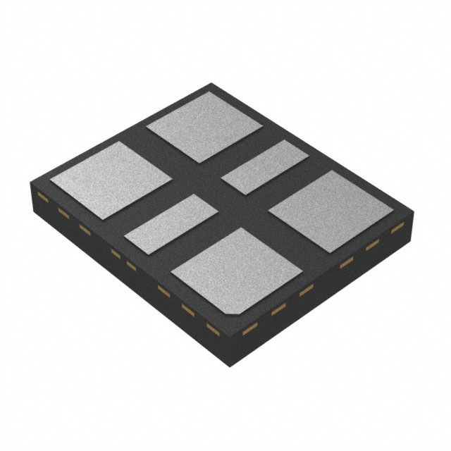
TBU-DB-Q Series - TBU® High-Speed Protectors
General Information
Additional Information
®
Click these links for more information:
®
The TBU-DB-Q Series of Bourns TBU products are
low capacitance dual bidirectional high-speed protection
components, constructed using MOSFET semiconductor
technology, and designed to protect against faults caused by
short circuits, overvoltage transients and faults in battery cells,
up to rated limits.
Line 1 I/O
1
3
Line 1 I/O
Line 2 I/O
6
4
Line 2 I/O
PRODUCT TECHNICAL INVENTORY SAMPLES
SELECTOR LIBRARY
TBU ® Device
CONTACT
The TBU® high-speed protector placed in the system circuit will monitor the current with the
MOSFET detection circuit triggering to provide an effective barrier behind which sensitive
electronics will not be exposed to large currents during transient events.
The TBU® device is provided in a surface mount DFN package and meets industry standard
requirements such as RoHS and Pb Free solder reflow profiles.
Absolute Maximum Ratings (@ TA = 25 °C Unless Otherwise Noted)
Symbol
Parameter
Value
Unit
Vimp
Peak impulse voltage withstand with duration less than 10 ms
550
V
Vdc
Peak DC voltage withstand with duration less than 1 hour
450
V
Top
Operating temperature range
-55 to +125
°C
Tstg
Storage temperature range
-65 to +150
°C
Tamax
Maximum Ambient Temperature
+125
°C
Electrical Characteristics (@ TA = 25 °C Unless Otherwise Noted)
Symbol
Parameter
Min.
Typ.
Max.
Unit
Itrigger
Current required for the device to go from operating state to
protected state
100
150
200
mA
Rdevice
Series resistance of the TBU® device
10.5
13.5
16.5
Ω
±0.5
Ω
®
®
Rmatch
Package resistance matching of the TBU device #1 - TBU device #2
tblock
Time taken for the device to go into current limiting
®
1
μs
0.5
mA
IQ
Current through the triggered TBU device with 50 Vdc circuit voltage
Vreset
Voltage below which the triggered TBU®
device will transition to normal operating state
Rth(j-a)
Junction to package pads - FR4 using JESD51-3 board
125
°C/W
Rth(j-a)
Junction to package pads - FR4 using JESD51-7 board
50
°C/W
4.5
7.5
9.5
V
Environmental Characteristics
Parameter
Moisture Sensitivity Level
ESD Classification (HBM)
Value
1
1B
*RoHS Directive 2015/863, Mar 31, 2015 and Annex.
**”Q” part number suffix for automotive and other applications requiring appropriate AEC-Q101 compliance.
Specifications are subject to change without notice.
Users should verify actual device performance in their specific applications.
The products described herein and this document are subject to specific legal disclaimers as set forth on the last page of this document, and at www.bourns.com/docs/legal/disclaimer.pdf.
�TBU-DB-Q Series - TBU® High-Speed Protectors
Reference Application
Basic TBU Operation
®
The TBU devices are general use protectors used in a wide
variety of applications, including telecommunications, industrial
communications and automotive battery management systems.
The maximum voltage rating of the TBU® device should never
be exceeded. Where necessary, an OVP device should be
employed to limit the maximum voltage. A cost-effective
protection solution combines Bourns® TBU® protection devices
with a pair of Bourns® TISP® Overvoltage Protectors or MOVs.
For bandwidth sensitive applications, a Bourns® GDT may be
substituted for the MOV.
Line
Side
1
3
6
4
OVP
Load
OVP
The TBU® device, constructed using MOSFET semiconductor
technology, placed in the system circuit will monitor the current
with the MOSFET detection circuit triggering to provide an
effective barrier behind which sensitive electronics are not
exposed to large voltages or currents during transient events.
When operated, the TBU® device will limit the current to less
than the Itrigger value within the tblock duration. If voltage
above Vreset is continuously sustained, the TBU® device will
subsequently reduce the current to a quiescent current level
within a period of time that is dependent upon the applied
voltage.
After the surge, the TBU® device resets when the voltage across
the TBU® device falls to the Vreset level. The TBU® device will
automatically reset on lines which have no DC bias or have DC
bias below Vreset (such as unpowered signal lines).
TBU ® Device
Specifications are subject to change without notice.
Users should verify actual device performance in their specific applications.
The products described herein and this document are subject to specific legal disclaimers as set forth on the last page of this document, and at www.bourns.com/docs/legal/disclaimer.pdf.
�TBU-DB-Q Series - TBU® High-Speed Protectors
Performance Graphs
Typical V-I Characteristics
Typical Trigger Current vs. Temperature
2.0
ITRIP
1.8
Normalized Trip Current
CURRENT
VRESET
VOLTAGE
1.6
1.4
1.2
1.0
0.8
0.6
0.4
0.2
0.0
-55
-35
-15
5
25
45
65
85
105
125
85
105
125
Junction Temperature (°C)
Power Derating Curve
Typical Resistance vs. Temperature
2.0
Multilayer JESD51-7 (2 TBU® HSPs)
Single Layer (2 TBU® HSPs)
Multilayer JESD51-7 (1 TBU® HSP)
Single Layer (1 TBU® HSP)
2.5
1.8
1.6
Normalized Resistance
Total Maximum Power (W)
3.0
2.0
1.5
1.0
0.5
1.4
1.2
1.0
0.8
0.6
0.4
0.2
0.0
25
45
65
85
105
Junction Temperature (°C)
125
145
0.0
-55
-35
-15
5
25
45
65
Junction Temperature (°C)
Specifications are subject to change without notice.
Users should verify actual device performance in their specific applications.
The products described herein and this document are subject to specific legal disclaimers as set forth on the last page of this document, and at www.bourns.com/docs/legal/disclaimer.pdf.
�TBU-DB-Q Series - TBU® High-Speed Protectors
Product Dimensions
TOP VIEW
G
SIDE VIEW 2
K
D
B
L
BXXXX
YWWLL
A
PIN 1 INDICATOR
DIMENSIONS:
Dim.
A
B
C
D
Min.
5.40
(.213)
6.40
(.252)
0.80
(.031)
0.00
(.000)
E
F
G
H
I
J
K
L
1.90
(.075)
1.75
(.069)
0.65
(.026)
0.70
(.028)
0.30
(.012)
0.25
(.010)
0.75
(.030)
Nom.
5.50
(.217)
6.50
(.256)
0.90
(.035)
—
Max.
5.60
(.220)
6.60
(.260)
1.00
(.039)
0.05
(.002)
0.20
REF.F
(.008) .......
2.00
(.079)
1.85
(.073)
0.70
(.028)
0.80
(.031)
0.35
(.014)
0.30
(.012)
0.80
(.031)
2.10
(.083)
1.95
(.077)
0.75
(.030)
0.90
(.035)
0.40
(.016)
0.35
(.014)
0.85
(.033)
5
6
3
2
1
F
E
C
SIDE VIEW 1
4
MM
(INCHES)
I
J
CHAMFERED
CORNER
FOR PIN 1
IDENTIFICATION
0.25 ± 0.25
(.010 ± .010)
H
Pad #
1
2
3
4
5
6
Pin Out
Line 1 In/Out
NU (Not Used)
Line 1 In/Out
L Line 2 In/Outt
NU (Not Used)
Line 2 In/Out
NOTES:
1. Pin 1 Indicator is laser marked; radius and location within the
Pin 1 terminal.
Pin 1 dot size: 0.500 ± 0.125 mm / .020 ± .005 in.
2. Pin 2 and 5 are NU (Not Used) and must be left unconnected;
do not connect to In/Out lines, do not connect to system Ground.
3. Coplanarity on exposed pads shall not exceed 0.08 mm / .003 in.
4. Warpage shall not exceed 0.10 mm / .004 in. on all surfaces.
5. Exposed tie bars at package side are not plated.
Specifications are subject to change without notice.
Users should verify actual device performance in their specific applications.
The products described herein and this document are subject to specific legal disclaimers as set forth on the last page of this document, and at www.bourns.com/docs/legal/disclaimer.pdf.
�TBU-DB-Q Series - TBU® High-Speed Protectors
Recommended Pad Layout
TBU® High-Speed Protectors have a 100 % matte-tin termination
finish. For improved thermal dissipation, the recommended layout
uses PCB copper areas which extend beyond the exposed solder
pad. The exposed solder pads should be defined by a solder
mask which matches the pad layout of the TBU® device in size
and spacing. It is recommended that they should be the same
dimension as the TBU® pads but if smaller solder pads are used,
they should be centered on the TBU® package terminal pads and
not more than 0.10-0.12 mm (0.004-0.005 in.) smaller in overall
width or length. Solder pad areas should not be larger than the
TBU® pad sizes to ensure adequate clearance is maintained. The
recommended stencil thickness is 0.10-0.12 mm (0.004-0.005 in.)
with a stencil opening size 0.025 mm (0.0010 in.) less than the
solder pad size. Extended copper areas beyond the solder pad
significantly improve the junction to ambient thermal resistance,
resulting in operation at lower junction temperatures with a
corresponding benefit of reliability. All pads should soldered to
the PCB, including pads marked as NC or NU but no electrical
connection should be made to these pads. Care should be
taken to assure no resistive path exists between the NU pins to
any other point to avoid unexpected performance issues. For
minimum parasitic capacitance, it is recommended that signal,
ground or power signals are not routed beneath any pad.
6
5
4
1
2
3
Dark grey areas show added PCB copper area for better
thermal resistance.
Reflow Profile
Profile Feature
Average Ramp-Up Rate (Tsmax to Tp)
Preheat
- Temperature Min. (Tsmin)
- Temperature Max. (Tsmax)
- Time (tsmin to tsmax)
Time maintained above:
- Temperature (TL)
- Time (tL)
Peak/Classification Temperature (Tp)
Time within 5 °C of Actual Peak Temp. (tp)
Ramp-Down Rate
Time 25 °C to Peak Temperature
Pb-Free Assembly
3 °C/sec. max.
150 °C
200 °C
60-180 sec.
217 °C
60-150 sec.
260 °C
20-40 sec.
6 °C/sec. max.
8 min. max.
How to Order
Typical Part Marking
TBU - DB 055 - 100 - WH - Q
MANUFACTURER’S
TRADEMARK
TBU® Product
Series
DB = Dual Bidirectional Series
BXXXX
YWWLL
Impulse Voltage Rating
055 = 550 V
Trigger Current
100 = 100 mA
Hold to Trip Ratio Suffix
W = Hold to Trip Ratio
PIN 1 INDICATOR
5 DIGIT PRODUCT CODE:
• 1ST ALPHA CHARACTER INDICATES PRODUCT FAMILY:
B = TBU-DB SERIES
• 2ND & 3RD DIGITS INDICATE IMPULSE VOLTAGE.
• 4TH & 5TH DIGITS INDICATE TRIGGER CURRENT.
UNDERSCORE DENOTES AEC-Q101 COMPLIANCE.
MANUFACTURING
DATE CODE:
• 1ST DIGIT INDICATES THE YEAR.
• 2ND & 3RD DIGITS INDICATE THE WEEK NUMBER.
• 4TH & 5TH DIGITS INDICATE LOT CODE.
Package Suffix
H = DFN Package
AEC-Q101 Suffix
Q = AEC-Q101 Compliant
Specifications are subject to change without notice.
Users should verify actual device performance in their specific applications.
The products described herein and this document are subject to specific legal disclaimers as set forth on the last page of this document, and at www.bourns.com/docs/legal/disclaimer.pdf.
�TBU-DB-Q Series - TBU® High-Speed Protectors
Packaging Specifications
P0
D
t
B
E
P2
TOP
COVER
TAPE
A
N
F
W
C
D
B0
K0
CENTER
LINES OF
CAVITY
A0
P
D1
EMBOSSMENT
G (MEASURED AT HUB)
USER DIRECTION OF FEED
QUANTITY: 3000 PIECES PER REEL
A
Min.
328.5
(12.93)
B
Max.
331
(13.05)
Min.
2.0
(0.079)
A0
Min.
5.75
(0.224)
C
Max.
2.4
(0.094)
B0
Max.
5.95
(0.234)
Min.
6.75
(0.266)
Min.
Max.
1.05
(0.041)
1.25
(0.049)
D
Max.
13.5
(.531)
D0
Max.
6.95
(0.274)
Min.
1.5
(0.059)
Min.
Max.
7.9
(0.311)
8.1
(0.319)
K0
Min.
12.8
(0.504)
Min.
17.0
(0.669)
D1
Min.
1.5
(0.059)
Min.
Max.
Min.
Max.
3.9
(0.159)
4.1
(0.161)
1.9
(0.075)
2.1
(0.083)
P0
G
Ref.
16.5
(0.650)
N
Ref.
100 ± 1.5
(3.94 ± 0.059)
E
Max.
1.6
(0.063)
P
Max.
17.4
(0.690)
Max.
—
Min.
1.65
(0.065)
F
Max.
1.85
(0.073)
Min.
7.4
(0.291)
Min.
Max.
Min.
Max.
0.25
(0.010)
0.35
(0.014)
15.7
(0.618)
16.3
(0.642)
P2
t
max.
7.6
(0.299)
W
DIMENSIONS:
MM
(INCHES)
Asia-Pacific: Tel: +886-2 2562-4117 • Email: asiacus@bourns.com
EMEA: Tel: +36 88 885 877 • Email: eurocus@bourns.com
The Americas: Tel: +1-951 781-5500 • Email: americus@bourns.com
www.bourns.com
REV. 11/21
“TBU” is a registered trademark of Bourns, Inc. in the United States and other countries, except Japan. All references to TBU® in this document for use in Japan shall be deemed to be
replaced with Bourns® TBU™.
Specifications are subject to change without notice.
Users should verify actual device performance in their specific applications.
The products described herein and this document are subject to specific legal disclaimers as set forth on the last page of this document, and at www.bourns.com/docs/legal/disclaimer.pdf.
�Legal Disclaimer Notice
This legal disclaimer applies to purchasers and users of Bourns® products manufactured by or on behalf of Bourns, Inc. and
P[Z�HɉSPH[LZ��JVSSLJ[P]LS`��¸)V\YUZ¹��
Unless otherwise expressly indicated in writing, Bourns® products and data sheets relating thereto are subject to change
^P[OV\[�UV[PJL���
很抱歉,暂时无法提供与“TBU-DB055-100-WH-Q”相匹配的价格&库存,您可以联系我们找货
免费人工找货- 国内价格 香港价格
- 1+35.923011+4.65055
- 10+23.5377910+3.04717
- 100+16.48531100+2.13417
- 500+13.50313500+1.74810
- 国内价格 香港价格
- 3000+11.280673000+1.46038
- 6000+11.031966000+1.42819
- 国内价格
- 1+26.10006
- 10+18.60183
- 50+15.64327
- 100+15.09228